EA-QSB-110 Embedded Artists, EA-QSB-110 Datasheet - Page 16
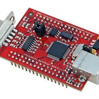
EA-QSB-110
Manufacturer Part Number
EA-QSB-110
Description
MCU, MPU & DSP Development Tools QUICKSTART PROTOTYPE BRD W/ LPC2148
Manufacturer
Embedded Artists
Specifications of EA-QSB-110
Processor To Be Evaluated
LPC2148
Data Bus Width
16 bit, 32 bit
Interface Type
RS-232, USB, I2C, SPI, UART
Core
ARM7TDMI-S
Dimensions
59 mm x 39.5 mm
Maximum Operating Temperature
+ 85 C
Operating Supply Voltage
5 V
Lead Free Status / RoHS Status
Lead free / RoHS Compliant


NXP Semiconductors
LPC2141_42_44_46_48_4
Product data sheet
6.7.1 Features
6.8.1 Features
6.9.1 Features
6.7 Fast general purpose parallel I/O (GPIO)
6.8 10-bit ADC
6.9 10-bit DAC
Device pins that are not connected to a specific peripheral function are controlled by the
GPIO registers. Pins may be dynamically configured as inputs or outputs. Separate
registers allow setting or clearing any number of outputs simultaneously. The value of the
output register may be read back, as well as the current state of the port pins.
LPC2141/42/44/46/48 introduce accelerated GPIO functions over prior LPC2000 devices:
The LPC2141/42 contain one and the LPC2144/46/48 contain two analog to digital
converters. These converters are single 10-bit successive approximation analog to digital
converters. While ADC0 has six channels, ADC1 has eight channels. Therefore, total
number of available ADC inputs for LPC2141/42 is 6 and for LPC2144/46/48 is 14.
The DAC enables the LPC2141/42/44/46/48 to generate a variable analog output. The
maximum DAC output voltage is the VREF voltage.
•
•
•
•
•
•
•
•
•
•
•
•
•
•
•
•
•
•
GPIO registers are relocated to the ARM local bus for the fastest possible I/O timing.
Mask registers allow treating sets of port bits as a group, leaving other bits
unchanged.
All GPIO registers are byte addressable.
Entire port value can be written in one instruction.
Bit-level set and clear registers allow a single instruction set or clear of any number of
bits in one port.
Direction control of individual bits.
Separate control of output set and clear.
All I/O default to inputs after reset.
10 bit successive approximation analog to digital converter.
Measurement range of 0 V to VREF (2.0 V
Each converter capable of performing more than 400000 10-bit samples per second.
Every analog input has a dedicated result register to reduce interrupt overhead.
Burst conversion mode for single or multiple inputs.
Optional conversion on transition on input pin or timer match signal.
Global Start command for both converters (LPC2142/44/46/48 only).
10-bit DAC.
Buffered output.
Power-down mode available.
Rev. 04 — 17 November 2008
LPC2141/42/44/46/48
Single-chip 16-bit/32-bit microcontrollers
VREF
V
DDA
).
© NXP B.V. 2008. All rights reserved.
16 of 40
Related parts for EA-QSB-110
Image
Part Number
Description
Manufacturer
Datasheet
Request
R

Part Number:
Description:
MCU, MPU & DSP Development Tools QUICKSTART PROTOTYPE BRD W/ LPC2129 CAN
Manufacturer:
Embedded Artists
Datasheet:

Part Number:
Description:
MCU, MPU & DSP Development Tools QUICKSTART PROTOTYPE BRD
Manufacturer:
Embedded Artists
Datasheet:

Part Number:
Description:
MCU, MPU & DSP Development Tools LPC2148 USB QUICKSTART BRD
Manufacturer:
Embedded Artists
Datasheet:

Part Number:
Description:
MCU, MPU & DSP Development Tools QUICKSTART PROTOTYPE BRD W/ LPC2106 RS232
Manufacturer:
Embedded Artists
Datasheet:
Part Number:
Description:
MCU, MPU & DSP Development Tools LPC2129 CAN QUICKSTART BRD
Manufacturer:
Embedded Artists
Datasheet:
Part Number:
Description:
MCU, MPU & DSP Development Tools LPC2106 RS232 QUICKSTART BRD
Manufacturer:
Embedded Artists
Datasheet:

Part Number:
Description:
BOARD QUICK START LPC1343
Manufacturer:
Embedded Artists
Datasheet:

Part Number:
Description:
Development Boards & Kits - ARM QUICK START BOARD LPC11U35
Manufacturer:
Embedded Artists
Datasheet:
Part Number:
Description:
KIT LPC3141 SODIMM 66X48 200POS
Manufacturer:
Embedded Artists
Datasheet:
Part Number:
Description:
KIT LPC3152 SODIMM 66X48 200POS
Manufacturer:
Embedded Artists
Datasheet:
Part Number:
Description:
BOARD OEM W/LPC2478 MCU
Manufacturer:
Embedded Artists
Datasheet:
Part Number:
Description:
KIT LPC3250 259 WITH QVGA
Manufacturer:
Embedded Artists
Datasheet: