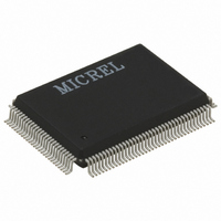
KSZ8995MI Micrel Inc, KSZ8995MI Datasheet - Page 36

KSZ8995MI
Manufacturer Part Number
KSZ8995MI
Description
5 Port 10/100 Switch With PHY And Frame Buffers
Manufacturer
Micrel Inc
Specifications of KSZ8995MI
Applications
*
Mounting Type
Surface Mount
Package / Case
128-MQFP, 128-PQFP
Number Of Primary Switch Ports
5
Internal Memory Buffer Size
64
Operating Supply Voltage (typ)
1.8/2.5/3.3V
Fiber Support
Yes
Integrated Led Drivers
Yes
Phy/transceiver Interface
MII/SNI
Power Supply Type
Analog/Digital
Package Type
PQFP
Data Rate (typ)
10/100Mbps
Vlan Support
Yes
Operating Temperature (max)
85C
Operating Temperature (min)
-40C
Pin Count
128
Mounting
Surface Mount
Jtag Support
No
Operating Supply Voltage (max)
1.9/2.6/3.6V
Operating Supply Voltage (min)
1.7/2.4/3V
Operating Temperature Classification
Industrial
Data Rate
100Mbps
Lead Free Status / RoHS Status
Lead free / RoHS Compliant
Other names
576-2127
KSZ8995MI
KSZ8995MI
Available stocks
Company
Part Number
Manufacturer
Quantity
Price
KS8995M
To use the KS8995M SPI:
M9999-062309
1. At the board level, connect KS8995M pins as follows:
KS8995M
Pin Number
112
110
111
109
2. Set the input signals PS[1:0] (pins 113 and 114 respectively) to “10” to set the serial configuration to SPI slave mode.
3. Power up the board and assert a reset signal. After reset, the start switch bit in register 1 will be set to ‘0’. Configure
4. Write configuration to registers using a typical SPI write data cycle as shown in Figure 8 or SPI multiple write as shown
5. Registers can be read and configuration can be verified with a typical SPI read data cycle as shown in Figure 9 or
6. After configuration is written and verified, write a ‘1’ to register 1 bit 0 to begin KS8995M operation.
the desired settings in the KS8995M before setting the start register to ‘1’.
in Figure 10. Note that data input on SPID is registered on the rising edge of SPIC.
a multiple read as shown in Figure 11. Note that read data is registered out of SPIQ on the falling edge of SPIC.
KS8995M
Signal Name
SPIS_N
SPIC
SPID
SPIQ
Table 9. SPI Connections
Microprocessor Signal
Description
SPI Slave Select
SPI Clock
Master Out Slave Input
Master In Slave Output
36
Micrel, Inc.
June 2009


