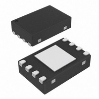
24AA16HT-I/MNY Microchip Technology, 24AA16HT-I/MNY Datasheet - Page 6

24AA16HT-I/MNY
Manufacturer Part Number
24AA16HT-I/MNY
Description
16K, 2K X 8 1.8V SERIAL EE, IND, 1/2 ARRAY WP 8 TDFN 2x3x0.8mm T/R
Manufacturer
Microchip Technology
Datasheet
1.24LC16BHT-IOT.pdf
(28 pages)
Specifications of 24AA16HT-I/MNY
Format - Memory
EEPROMs - Serial
Memory Type
EEPROM
Memory Size
16K (2K x 8)
Speed
100kHz, 400kHz
Interface
I²C, 2-Wire Serial
Voltage - Supply
1.7 V ~ 5.5 V
Operating Temperature
-40°C ~ 85°C
Package / Case
8-TDFN
Lead Free Status / RoHS Status
Lead free / RoHS Compliant
Other names
24AA16HT-I/MNYTR
24AA16H/24LC16BH
3.6
A control byte is the first byte received following the
Start condition from the master device (Figure 3-2).
The control byte consists of a four-bit control code. For
the 24XX16H, this is set as ‘
write operations. The next three bits of the control byte
are the block-select bits (B2, B1, B0). They are used by
the master device to select which of the eight 256 word-
blocks of memory are to be accessed. These bits are in
effect the three Most Significant bits of the word
address.
The last bit of the control byte defines the operation to
be performed. When set to ‘
selected. When set to ‘
Following the Start condition, the 24XX16H monitors
the SDA bus, checking the device type identifier being
transmitted and, upon receiving a ‘
slave device outputs an Acknowledge signal on the
SDA line. Depending on the state of the R/W bit, the
24XX16H will select a read or write operation.
DS22118A-page 6
Operation
Read
Write
Device Addressing
Control
1010
1010
Code
0
’ a write operation is selected.
1010’
Block Address
Block Address
Block Select
1
’ a read operation is
binary for read and
1010’
code, the
R/W
1
0
FIGURE 3-2:
Start Bit
S
1
Control Code
0
Slave Address
1
CONTROL BYTE
ALLOCATION
0
© 2008 Microchip Technology Inc.
B2 B1 B0 R/W ACK
Select
Block
Bits
Acknowledge Bit
Read/Write Bit


