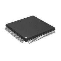
AD5383BSTZ-3 Analog Devices Inc, AD5383BSTZ-3 Datasheet - Page 10

AD5383BSTZ-3
Manufacturer Part Number
AD5383BSTZ-3
Description
32-Chn 3V Single Supply 12-Bit Vout I.C.
Manufacturer
Analog Devices Inc
Datasheet
1.AD5383BSTZ-5.pdf
(40 pages)
Specifications of AD5383BSTZ-3
Design Resources
32 Channels of Programmable Voltage with Excellent Temperature Drift Performance Using AD5383 (CN0014) AD5383 Channel Monitor Function (CN0015)
Settling Time
6µs
Number Of Bits
12
Data Interface
Serial, Parallel
Number Of Converters
32
Voltage Supply Source
Single Supply
Power Dissipation (max)
39mW
Operating Temperature
-40°C ~ 85°C
Mounting Type
Surface Mount
Package / Case
100-LQFP
Lead Free Status / RoHS Status
Lead free / RoHS Compliant
Available stocks
Company
Part Number
Manufacturer
Quantity
Price
Company:
Part Number:
AD5383BSTZ-3
Manufacturer:
Analog Devices Inc
Quantity:
10 000
Part Number:
AD5383BSTZ-3
Manufacturer:
ADI/亚德诺
Quantity:
20 000
AD5383
I
DV
noted.
Table 7.
Parameter
F
t
t
t
t
t
t
t
t
t
t
t
C
1
2
3
4
1
2
3
4
5
6
7
8
9
10
11
2
Guaranteed by design and characterization, not production tested.
See Figure 6.
A master device must provide a hold time of at least 300 ns for the SDA signal (referred to the V
falling edge.
C
SCL
b
3
SDA
C SERIAL INTERFACE TIMING
SCL
b
is the total capacitance, in pF, of one bus line. t
DD
= 2.7 V to 5.5 V; AV
1, 2
t
9
CONDITION
Limit at T
400
2.5
0.6
1.3
0.6
100
0.9
0
0.6
0.6
1.3
300
0
300
0
300
20 + 0.1 C
400
START
t
4
DD
MIN
b
4
= 4.5 V to 5.5 V or 2.7 V to 3.6 V; AGND = DGND = 0 V; all specifications T
t
3
, T
MAX
t
R
10
kHz max
ns min
ns min
pF max
Unit
μs min
μs min
μs min
μs min
ns min
μs max
μs min
μs min
μs min
μs min
ns max
ns max
ns max
ns min
and t
t
6
Figure 6. I
F
are measured between 0.3 DV
2
C-Compatible Serial Interface Timing Diagram
t
2
Rev. B | Page 10 of 40
Description
SCL clock frequency
SCL cycle time
t
t
t
t
t
t
t
t
t
t
t
t
t
t
t
Capacitive load for each bus line
HIGH
LOW
HD,STA
SU,DAT
HD,DAT
HD,DAT
SU,STA
SU,STO
BUF
R
R
F
F
F
F
, rise time of SCL and SDA when receiving
, rise time of SCL and SDA when receiving (CMOS-compatible)
, fall time of SDA when transmitting
, fall time of SDA when receiving (CMOS-compatible)
, fall time of SCL and SDA when receiving
, fall time of SCL and SDA when transmitting
t
11
, bus free time between a STOP and a START condition
, SCL low time
, SCL high time
, setup time for repeated start
, start/repeated start condition hold time
, data setup time
, stop condition setup time
t
, data hold time
, data hold time
5
DD
and 0.7 DV
IH
min of the SCL signal) in order to bridge the undefined region of SCL’s
DD
.
CONDITION
REPEATED
START
t
7
t
4
t
MIN
1
to T
MAX
, unless otherwise
CONDITION
STOP
t
8


