AD5532ABC-2 Analog Devices Inc, AD5532ABC-2 Datasheet

IC,Sample/Track-and-Hold Amplifier,32-CHANNEL,CMOS,BGA,74PIN,PLASTIC

AD5532ABC-2

Manufacturer Part Number
AD5532ABC-2
Description
IC,Sample/Track-and-Hold Amplifier,32-CHANNEL,CMOS,BGA,74PIN,PLASTIC
Manufacturer
Analog Devices Inc
Datasheets

Specifications of AD5532ABC-2

Rohs Status
RoHS non-compliant
Settling Time
30µs
Number Of Bits
14
Data Interface
Serial
Number Of Converters
34
Voltage Supply Source
Analog and Digital
Power Dissipation (max)
623mW
Operating Temperature
-40°C ~ 85°C
Mounting Type
Surface Mount
Package / Case
74-CSPBGA
Number Of Channels
32
Resolution
14b
Conversion Rate
45KSPS
Interface Type
PARALLEL/SERIAL 3W
Single Supply Voltage (typ)
Not RequiredV
Dual Supply Voltage (typ)
±9/5/±12/5/±15/5V
Power Supply Requirement
Dual
Output Type
Voltage
Single Supply Voltage (min)
Not RequiredV
Single Supply Voltage (max)
Not RequiredV
Dual Supply Voltage (min)
-4.75/8/4.75V
Dual Supply Voltage (max)
±16.5/5.25V
Operating Temp Range
-40C to 85C
Operating Temperature Classification
Industrial
Mounting
Surface Mount
Pin Count
74
For Use With
EVAL-AD5532HSEBZ - BOARD EVAL FOR AD5532HSEVAL-AD5532EBZ - BOARD EVAL FOR AD5532
Lead Free Status / Rohs Status
Not Compliant

Available stocks

Company
Part Number
Manufacturer
Quantity
Price
Part Number:
AD5532ABC-2
Manufacturer:
AD
Quantity:
1 831
Part Number:
AD5532ABC-2
Manufacturer:
ADI
Quantity:
150
Part Number:
AD5532ABC-2
Manufacturer:
Analog Devices Inc
Quantity:
10 000
a
*Protected by U.S. Patent No. 5,969,657
REV. A
Information furnished by Analog Devices is believed to be accurate and
reliable. However, no responsibility is assumed by Analog Devices for its
use, nor for any infringements of patents or other rights of third parties that
may result from its use. No license is granted by implication or otherwise
under any patent or patent rights of Analog Devices. Trademarks and
registered trademarks are the property of their respective companies.
FEATURES
Infinite Sample-and-Hold Capability to
High Integration:
Per Channel Acquisition Time of 16 s Max
Adjustable Voltage Output Range
Output Impedance 0.5
Output Voltage Span 10 V
Readback Capability
DSP/Microcontroller Compatible Serial Interface
Parallel Interface
Temperature Range –40 C to +85 C
APPLICATIONS
Optical Networks
Automatic Test Equipment
Level Setting
Instrumentation
Industrial Control Systems
Data Acquisition
Low Cost I/O
32-Channel DAC in 12 mm
TRACK / RESET
DAC GND
SER / PAR
DGND
AGND
BUSY
.
V
12 mm CSPBGA
IN
AD5533
SCLK
0.018% Accuracy
INTERFACE
CONTROL
FUNCTIONAL BLOCK DIAGRAM
DV
LOGIC
D
CC
IN
ADC
AV
D
OUT
CC
REF IN REF OUT
SYNC/ CS
DAC
DAC
DAC
GENERAL DESCRIPTION
The AD5533 combines a 32-channel voltage translation function
with an infinite output hold capability. An analog input voltage
on the common input pin, V
sentation transferred to a chosen DAC Register. V
DAC is then updated to reflect the new contents of the DAC
register. Channel selection is accomplished via the parallel address
inputs A0–A4 or via the serial input port. The output voltage
range is determined by the offset voltage at the OFFS_IN pin
and the gain of the output amplifier. It is restricted to a range
from V
output amplifier.
The device is operated with AV
and requires a stable 3 V reference on REF_IN as well as an
offset voltage on OFFS_IN.
PRODUCT HIGHLIGHTS
1. Infinite Droopless Sample-and-Hold Capability.
2. The AD5533 is available in a 74-lead CSPBGA with a body
+5.25 V, V
One Technology Way, P.O. Box 9106, Norwood, MA 02062-9106, U.S.A.
Tel: 781/329-4700
Fax: 781/326-8703
ADDRESS INPUT REGISTER
size of 12 mm
A4 –A0
SS
OFFS IN
+ 2 V to V
SS
CAL
= –4.75 V to –16.5 V, and V
OFFSET SEL
V
DD
DD
12 mm.
© 2003 Analog Devices, Inc. All rights reserved.
– 2 V because of the headroom of the
V
SS
32-Channel Infinite
IN
Sample-and-Hold
CC
, is sampled and its digital repre-
V
V
OFFS OUT
WR
OUT
OUT
= +5 V ± 5%, DV
0
31
DD
AD5533
= +8 V to +16.5 V
www.analog.com
CC
OUT
= +2.7 V to
for this
*

Related parts for AD5532ABC-2

AD5532ABC-2 Summary of contents

Page 1

FEATURES Infinite Sample-and-Hold Capability to High Integration: 32-Channel DAC CSPBGA Per Channel Acquisition Time Max Adjustable Voltage Output Range Output Impedance 0.5 Output Voltage Span 10 V Readback Capability DSP/Microcontroller Compatible ...

Page 2

AD5533 –SPECIFICATIONS – All outputs unloaded. All specifications Parameter ANALOG CHANNEL Nonlinearity IN OUT Gain Offset Error ANALOG INPUT ( Input Voltage Range ...

Page 3

Parameter POWER REQUIREMENTS Power Supply Voltages Power Supply Currents Power Dissipation NOTES 1 See Terminology Version: Industrial temperature range ...

Page 4

AD5533 TIMING CHARACTERISTICS PARALLEL INTERFACE Limit MIN 1, 2 Parameter (A Version NOTES 1 See Interface Timing Diagram. ...

Page 5

SERIAL INTERFACE TIMING DIAGRAMS t 1 SCLK SYNC MSB Figure 3. 10-Bit Write (ISHA Mode and Both Readback Modes SCLK SYNC t t ...

Page 6

... Time at Peak Temperature . . . . . . . . . . . . 10 sec to 40 sec Model Function AD5533ABC-1 32-Channel ISHA Only AD5533ABC-1REEL 32-Channel ISHA Only AD5533BBC-1* 32-Channel Precision ISHA Only AD5532ABC-1* 32 DACs, 32-Channel ISHA AD5532ABC-2* 32 DACs, 32-Channel ISHA AD5532ABC-3* 32 DACs, 32-Channel ISHA AD5532ABC-5* 32 DACs, 32-Channel ISHA AD5532BBC-1* 32 DACs, 32-Channel Precision ISHA AD5532HS* 32-Channel High-Speed DAC ...

Page 7

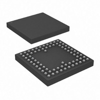
CSPBGA Ball Number Name A1 N CS/SYNC SCLK A8 OFFSET_SEL BUSY A9 TRACK/RESET A10 A11 N VO16 B2 N ...

Page 8

AD5533 Pin Function AGND(1–2) Analog GND Pins AV (1–2) Analog Supply Pins. Voltage range from 4. 5. (1–4) V Supply Pins. Voltage range from 16 (1–4) V Supply ...

Page 9

TERMINOLOGY Nonlinearity IN OUT This is a measure of the maximum deviation from a straight line passing through the endpoints of the V IN function expressed as a percentage of the full-scale span. Offset Error ...

Page 10

AD5533–Typical Performance Characteristics 0.0024 0.0020 REFIN 0.0016 OFFS_IN 0.0012 0.0008 0.0004 0.0000 –0.0004 –0.0008 –0.0012 –0.0016 –0.0020 –0.0024 0.1 V – TPC Accuracy ...

Page 11

FUNCTIONAL DESCRIPTION The AD5533 can be thought of as consisting of an ADC and 32 DACs in a single package. The input voltage V and converted into a digital word. The digital result is loaded into one of the DAC ...

Page 12

AD5533 Reset Function The reset function on the AD5533 can be used to reset all nodes on this device to their power-on-reset condition. This is imple- mented by applying a low-going pulse of between 90 ns and 200 ns to ...

Page 13

MSB 0 MODE BIT 1 MSB 1 0 MODE BITS b. Input Serial Interface (Acquire and Readback Mode) MSB 1 1 MODE BITS The serial interface is designed to allow easy interfacing to most microcontrollers and DSPs, e.g., PIC16C, PIC17C, ...

Page 14

AD5533 MICROPROCESSOR INTERFACING AD5533 to ADSP-21xx Interface The ADSP-21xx family of DSPs are easily interfaced to the AD5533 without the need for extra logic. A data transfer is initiated by writing a word to the Tx Register after the SPORT ...

Page 15

APPLICATION CIRCUITS AD5533 in a Typical ATE System The AD5533 infinite sample-and-hold is ideally suited for use in automatic test equipment. Several ISHAs are required to control pin drivers, comparators, active loads, and signal timing. Traditionally, sample-and-hold devices with droop ...

Page 16

AD5533 A1 1.70 MAX Revision History Location 7/03—Data Sheet changed from REV REV. A. Term SHA changed to ISHA . . . . . . . . . . . . . . . . . . . ...

Related keywords