AD557JP Analog Devices Inc, AD557JP Datasheet - Page 3
AD557JP
Manufacturer Part Number
AD557JP
Description
D/A Converter (D-A) IC
Manufacturer
Analog Devices Inc
Series
DACPORT®r
Datasheet
1.AD557JNZ.pdf
(6 pages)
Specifications of AD557JP
No. Of Bits
8 Bit
Mounting Type
Surface Mount
Interface Type
Parallel
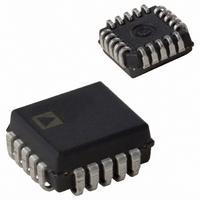
Package / Case
20-PLCC
Rohs Status
RoHS non-compliant
Settling Time
800ns
Number Of Bits
8
Data Interface
Parallel
Number Of Converters
1
Voltage Supply Source
Single Supply
Power Dissipation (max)
125mW
Operating Temperature
0°C ~ 70°C
Lead Free Status / RoHS Status
Available stocks
Company
Part Number
Manufacturer
Quantity
Price

Part Number:
AD557JP
Manufacturer:
ADI/亚德诺
Quantity:
20 000
Company:
Part Number:
AD557JP-REEL
Manufacturer:
Analog Devices Inc
Quantity:
10 000
Company:
Part Number:
AD557JP-REEL7
Manufacturer:
Analog Devices Inc
Quantity:
10 000
Company:
Part Number:
AD557JPZ
Manufacturer:
Analog Devices Inc
Quantity:
135
Part Number:
AD557JPZ
Manufacturer:
ADI/亚德诺
Quantity:
20 000
Company:
Part Number:
AD557JPZ-REEL
Manufacturer:
Analog Devices Inc
Quantity:
10 000


CIRCUIT DESCRIPTION
The AD557 consists of four major functional blocks fabricated
on a single monolithic chip (see Figure 1). The main D/A con-
verter section uses eight equally weighted laser-trimmed current
sources switched into a silicon-chromium thin-film R/2R resistor
ladder network to give a direct but unbuffered 0 mV to 400 mV
output range. The transistors that form the DAC switches are
PNPs; this allows direct positive-voltage logic interface and a
zero-based output range.
The high-speed output buffer amplifier is operated in the nonin-
verting mode with gain determined by the user-connections
at the output range select pin. The gain-setting application
resistors are thin film laser trimmed to match and track the
DAC resistors and to assure precise initial calibration of the out-
put range, 0 V to 2.56 V. The amplifier output stage is an
NPN transistor with passive pull-down for zero-based output
capability with a single power supply.
The internal precision voltage reference is of the patented
band-gap type. This design produces a reference voltage of
1.2 V and thus, unlike 6.3 V temperature-compensated Zeners,
may be operated from a single, low-voltage logic power supply.
The microprocessor interface logic consists of an 8-bit data
latch and control circuitry. Low power, small geometry and high
speed are advantages of the I
I
analog sections need not be compromised to provide on-chip
logic capabilities. The control logic allows the latches to be
operated from a decoded microprocessor address and write sig-
nal. If the application does not involve a µP or data bus, wiring
CS and CE to ground renders the latches “transparent” for
direct DAC access.
2
Binary
0000 0000
0000 0001
0000 0010
0000 1111
0001 0000
0111 1111
1000 0000
1100 0000
1111 1111
L is bipolar process compatible so that the performance of the
REFERENCE
BAND-GAP
CONTROL
CONTROL
CS CE
INPUTS
LOGIC
l
2
Digital Input Code
L
CONTROL
Hexadecimal
AMP
00
01
02
0F
10
7F
80
C0
FF
(MSB)
BIT1
DIGITAL INPUT DATA (BUS)
8-BIT VOLTAGE-SWITCHING
D-TO-A CONVERTER
2
L design as applied to this section.
l
2
L LATCHES
Decimal
0
1
2
15
16
127
128
192
255
(LSB)
BIT8
+ V
CC
OUTPUT
V
V
AMP
GND
OUT
OUT
Output
Voltage
0
0.010 V
0.020 V
0.150 V
0.160 V
1.270 V
1.280 V
1.920 V
2.55 V
SENSE A
SENSE B
GND
V
OUT
CONNECTING THE AD557
The AD557 has been configured for low cost and ease of appli-
cation. All reference, output amplifier and logic connections are
made internally. In addition, all calibration trims are performed
at the factory assuring specified accuracy without user trims.
The only connection decision to be made by the user is whether
the output range desired is unipolar or bipolar. Clean circuit
board layout is facilitated by isolating all digital bit inputs on
one side of the package; analog outputs are on the opposite side.
UNIPOLAR 0 V TO 2.56 V OUTPUT RANGE
Figure 2 shows the configuration for the 0 V to 2.56 V full-
scale output range. Because of its precise factory calibration, the
AD557 is intended to be operated without user trims for gain
and offset; therefore, no provisions have been made for such user
trims. If a small increase in scale is required, however, it may be
accomplished by slightly altering the effective gain of the output
buffer. A resistor in series with V
output range. Note that decreasing the scale by putting a resistor
in series with GND will not work properly due to the code-
dependent currents in GND. Adjusting offset by injecting dc at
GND is not recommended for the same reason.
BIPOLAR –1.28 V TO +1.28 V OUTPUT RANGE
The AD557 was designed for operation from a single power
supply and is thus capable of providing only a unipolar 0 V to
2.56 V output range. If a negative supply is available, bipolar
output ranges may be achieved by suitable output offsetting and
scaling. Figure 3 shows how a ± 1.28 V output range may be
achieved when a –5 V power supply is available. The offset is
provided by the AD589 precision 1.2 V reference which will
operate from a 5 V supply. The AD711 output amplifier can
provide the necessary ± 1.28 V output swing from ± 5 V supplies.
Coding is complementary offset binary.
AD557
V
IN
AD589
0.01 F
V
OUTPUT
–5V
OUT
AMP
–1.2V
4.7k
BIPOLAR
OFFSET
ADJUST
= 0V TO 2.56V
5k
500
4.53k
16
15
14
13
OUT
INPUT CODE
0 0 0 0 0 0 0 0
1 0 0 0 0 0 0 0
1 1 1 1 1 1 1 1
1.5k
AD711
V
V
OUT
OUT
GND
SENSE will increase the
V
SENSE A
SENSE B
OUT
+5V
–5V
5k
0.01 F
0.01 F
V
+1.28V
0V
–1.27V
OUT
±
AD557
+1.28 TO
–1.27
V
O
Related parts for AD557JP
Image
Part Number
Description
Manufacturer
Datasheet
Request
R

Part Number:
Description:
DPG2 EVAL ADAPTER FOR XILINX BOARDS
Manufacturer:
Analog Devices Inc
Part Number:
Description:
Xilinx FMC Interface
Manufacturer:
Analog Devices Inc
Datasheet:
Part Number:
Description:
Xilinx FMC Interface
Manufacturer:
Analog Devices Inc
Datasheet:
Part Number:
Description:
Xilinx FMC Interface
Manufacturer:
Analog Devices Inc
Datasheet:
Part Number:
Description:
Xilinx FMC Interface
Manufacturer:
Analog Devices Inc
Datasheet:
Part Number:
Description:
Xilinx FMC Interface
Manufacturer:
Analog Devices Inc
Datasheet:
Part Number:
Description:
Xilinx FMC Interface
Manufacturer:
Analog Devices Inc
Datasheet:
Part Number:
Description:
Xilinx FMC Interface
Manufacturer:
Analog Devices Inc
Datasheet:
Part Number:
Description:
AD CONVERTOR, IC, BIT COUNT FOR PROCESSOR
Manufacturer:
Analog Devices Inc

Part Number:
Description:
±1.7g Dual-Axis IMEMS Accelerometer Evaluation Board
Manufacturer:
Analog Devices Inc
Datasheet:
Part Number:
Description:
Inertial Sensor Evaluation System
Manufacturer:
Analog Devices Inc
Datasheet:
Part Number:
Description:
Manufacturer:
Analog Devices Inc
Datasheet: