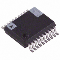
AD5726YRSZ-1REEL Analog Devices Inc, AD5726YRSZ-1REEL Datasheet - Page 14

AD5726YRSZ-1REEL
Manufacturer Part Number
AD5726YRSZ-1REEL
Description
Quad 12Bit DAC 0.5 LSB INL SERIAL
Manufacturer
Analog Devices Inc
Datasheet
1.AD5726YRSZ-REEL.pdf
(20 pages)
Specifications of AD5726YRSZ-1REEL
Settling Time
9µs
Number Of Bits
12
Data Interface
Serial
Number Of Converters
4
Voltage Supply Source
Dual ±
Power Dissipation (max)
30mW Unipolar; 240mW Bipolar
Operating Temperature
-40°C ~ 125°C
Mounting Type
Surface Mount
Package / Case
20-SSOP
Lead Free Status / RoHS Status
Lead free / RoHS Compliant
AD5726
SERIAL INTERFACE
The AD5726 is controlled over a versatile 3-wire serial interface
that operates at clock rates up to 30 MHz and is compatible with
SPI, QSPI™, MICROWIRE™, and DSP standards.
Input Shift Register
The input shift register is 16 bits wide. Data is loaded into the
device MSB first as a 16-bit word under the control of a serial
clock input, SCLK. The input register consists of two address
bits, two don’t care bits, and 12 data bits as shown in Table 10.
The timing diagram for this operation is shown in Figure 2.
When CS is low, the data presented to the input, SDIN, is shifted
MSB first into the internal shift register on the rising edge of
SCLK. Once all 16 bits of the serial data-word have been input,
the load control LDAC is strobed, and the word is latched onto
the internal data bus. The two address bits are decoded and used to
route the 12-bit data-word to the appropriate DAC data register.
Operation of CS and SCLK
The CS and SCLK pins are internally fed to the same logical OR
gate and, therefore, require careful attention during a load cycle
to avoid clocking in false data bits. As shown in the timing diagram
in
high, during the last high portion of SCLK following the rising
edge that clocked in the last data bit. Otherwise, an additional
rising edge is generated by CS rising while SCLK is low, causing
CS to act as the clock and allowing a false data bit into the input
shift register. The same must also be considered for the beginning
of the data load sequence.
Coding
The AD5726 uses binary coding. The output voltage can be
calculated from the following equation:
where D is the digital code in decimal.
Table 10. Input Register Format
DB0
A1
Figure 2
V
OUT
DB1
A0
, SCLK must be halted high, or
=
V
REFN
DB2
X
+
(
V
REFP
DB3
X
−
4096
V
REFN
DB4
D11
)
×
D
CS must be brought
DB5
D10
DB6
D9
DB7
D8
Rev. B | Page 14 of 20
DB8
D7
Load DAC ( LDAC )
When asserted, the LDAC pin is an asynchronous, active low,
digital input that transfers the contents of the input register to
the internal data bus, updating the addressed DAC output. New
data must not be programmed to the AD5726 while the LDAC
pin is low.
CLR and CLRSEL
The CLR control allows the user to perform an asynchronous
clear function. Asserting CLR loads all four DAC registers,
forcing the DAC outputs to either zero scale (0x000) or midscale
(0x800), depending on the state of CLRSEL as shown in
The
When CLR returns high, the DAC outputs remain at the clear
value until LDAC is strobed, reloading the individual DAC
registers with either the data held in the input register prior to
the clear or with new data loaded through the serial interface.
Table 8. CLR /CLRSEL Truth Table
CLR
0
0
1
1
Table 9. DAC Address Word Decode Table
A1
0
0
1
1
DB9
D6
CLR function is asynchronous and independent of CS .
DB10
D5
CLRSEL
0
1
0
1
A0
0
1
0
1
DB11
D4
DAC Addressed
DAC A
DAC B
DAC C
DAC D
DAC Registers
Zero scale (0x000)
Midscale (0x800)
No change
No change
DB12
D3
DB13
D2
DB14
D1
Table 8
DB15
D0
.


