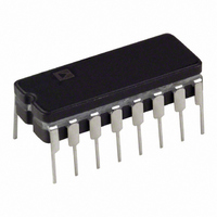
AD652SQ Analog Devices Inc, AD652SQ Datasheet - Page 16

AD652SQ
Manufacturer Part Number
AD652SQ
Description
IC,Voltage-to-Frequency Converter,DIP,16PIN
Manufacturer
Analog Devices Inc
Type
Voltage to Frequencyr
Datasheet
1.AD652JPZ.pdf
(28 pages)
Specifications of AD652SQ
Rohs Status
RoHS non-compliant
Frequency - Max
2MHz
Full Scale
±25ppm/°C
Linearity
±0.005%
Mounting Type
Through Hole
Package / Case
16-CDIP (0.300", 7.62mm)
Lead Free Status / RoHS Status
Available stocks
Company
Part Number
Manufacturer
Quantity
Price
Part Number:
AD652SQ
Manufacturer:
ADI/亚德诺
Quantity:
20 000
Company:
Part Number:
AD652SQ/883
Manufacturer:
TOS
Quantity:
6 223
AD652
DECOUPLING AND GROUNDING
supply-voltage pins, and to insert small valued resistors (10 Ω to
100 Ω) in the supply lines to provide a measure of decoupling
between the various circuits in a system. Ceramic capacitors of
0.1 µF to 1.0 µF should be applied between the supply voltage
pins and analog signal ground for proper bypassing on the
AD652.
Additionally, a larger board-level decoupling capacitor of 1 µF
to 10 µF should be located relatively close to the AD652 on each
power supply line. Such precautions are imperative in high
resolution data acquisition applications where one expects to
exploit the full linearity and dynamic range of the AD652.
Separate digital and analog grounds are provided on the AD652.
Only the emitter of the open-collector frequency output
transistor and the clock input threshold are returned to the
digital ground. Only the 5 V reference is connected to analog
ground. The purpose of the two separate grounds is to allow
isolation between the high precision analog signals and the
digital section of the circuitry. Much noise can be tolerated on
the digital ground without affecting the accuracy of the VFC.
Such ground noise is inevitable when switching the large
currents associated with the frequency output signal.
At high full-scale frequencies, it is necessary to use a pull-up
resistor of about 500 Ω in order to get the rise time fast enough
to provide well-defined output pulses. This means that from a
5 V logic supply, for example, the open collector output draws
10 mA. This much current being switched causes ringing on
long ground runs due to the self-inductance of the wires. For
instance, 20-gauge wire has an inductance of about 20 nH per
inch; a current of 10 mA being switched in 50 ns at the end of
12 inches of 20-gauge wire produces a voltage spike of 50 mV.
The separate digital ground of the AD652 easily handles these
types of switching transients.
It is good engineering practice to use bypass capacitors on the
Rev. C | Page 16 of 28
A problem remains from interference caused by radiation of
electromagnetic energy from these fast transients. Typically, a
voltage spike is produced by inductive switching transients;
these spikes can capacitively couple into other sections of the
circuit. Another problem is ringing of ground lines and power
supply lines due to the distributed capacitance and inductance
of the wires. Such ringing can also couple interference into
sensitive analog circuits. The best solution to these problems is
proper bypassing of the logic supply at the AD652 package. A
1 µF to 10 µF tantalum capacitor should be connected directly
to the supply side of the pull-up resistor and to the digital
ground, Pin 12. The pull-up resistor should be connected
directly to the frequency output, Pin 11. The lead lengths on the
bypass capacitor and the pull-up resistor should be as short as
possible. The capacitor supplies (or absorbs) the current
transients, and large ac signals flow in a physically small loop
through the capacitor, pull-up resistor, and frequency output
transistor. It is important that the loop be physically small for
two reasons: first, there is less inductance if the wires are short,
and second, the loop does not radiate RFI efficiently.
The digital ground (Pin 12) should be separately connected to
the power supply ground. Note that the leads to the digital
power supply are only carrying dc current. There may be a dc
ground drop due to the difference in currents returned on the
analog and digital grounds. This does not cause a problem;
these features greatly ease power distribution and ground
manage-ment in large systems. The proper technique for
grounding requires separate digital and analog ground returns
to the power supply. Also, the signal ground must be referred
directly to the analog ground (Pin 6) at the package. More
information on proper grounding and reduction of interference
can be found in Noise Reduction Techniques in Electronic
Systems , by H.W. Ort, (John Wiley, 1976).


