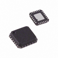
AD7147ACPZ-REEL Analog Devices Inc, AD7147ACPZ-REEL Datasheet - Page 38

AD7147ACPZ-REEL
Manufacturer Part Number
AD7147ACPZ-REEL
Description
IC,Converter, Other/Special/Miscellaneous,LLCC,24PIN
Manufacturer
Analog Devices Inc
Series
CapTouch™r
Type
Capacitive Sensor Controllerr
Datasheet
1.AD7147ACPZ-1500RL7.pdf
(72 pages)
Specifications of AD7147ACPZ-REEL
Resolution (bits)
16 b
Data Interface
Serial, SPI™
Voltage Supply Source
Single Supply
Voltage - Supply
2.6 V ~ 3.6 V
Operating Temperature
-40°C ~ 85°C
Mounting Type
Surface Mount
Package / Case
24-LFCSP
Lead Free Status / RoHS Status
Lead free / RoHS Compliant
For Use With
EVAL-AD7147EBZ - BOARD EVAL FOR AD7147ACPZEVAL-AD7147-1EBZ - BOARD EVAL FOR AD7147ACPZ-1
Sampling Rate (per Second)
-
Lead Free Status / Rohs Status
Compliant
AD7147
PCB DESIGN GUIDELINES
CAPACITIVE SENSOR BOARD MECHANICAL SPECIFICATIONS
Table 19.
Parameter
Distance from Edge of Any Sensor to Edge of Grounded Metal Object
Distance Between Sensor Edges
Distance Between Bottom of Sensor Board and Controller Board or Grounded
1
2
The distance is dependent on the application and the position of the switches relative to each other and with respect to the user’s finger position and handling.
Adjacent sensors with no space between them are implemented differentially.
The 1.0 mm specification is intended to prevent direct sensor board contact with any conductive material. This specification, however, does not guarantee an absence
of EMI coupling from the controller board to the sensors. To avoid potential EMI-coupling issues, place a grounded metal shield between the capacitive sensor board
and the main controller board, as shown in Figure 58.
Metal Casing
D
5
D
1
CONTROLLER PRINTED CIRCUIT BOARD OR METAL CASING
CAPACITIVE SENSOR
PRINTED CIRCUIT
Figure 57. Capacitive Sensor Board, Side View
Figure 56. Capacitive Sensor Board, Top View
SLIDER
2
CAPACITIVE SENSOR BOARD
METAL OBJECT
D
BUTTONS
2
1
SWITCH
8-WAY
D
D
4
3
Rev. B | Page 38 of 72
CHIP SCALE PACKAGES
The lands on the chip scale package (CP-24-3) are rectangular.
The PCB pad for these should be 0.1 mm longer than the package
land length and 0.05 mm wider than the package land width.
Center the land on the pad to maximize the solder joint size.
The bottom of the chip scale package has a central thermal pad.
The thermal pad on the printed circuit board should be at least
as large as this exposed pad. To avoid shorting, provide a clear-
ance of at least 0.25 mm between the thermal pad and the inner
edges of the land pattern on the PCB.
Thermal vias can be used on the PCB thermal pad to improve
the thermal performance of the package. If vias are used, they
should be incorporated in the thermal pad at a 1.2 mm pitch
grid. The via diameter should be between 0.3 mm and 0.33 mm,
and the via barrel should be plated with 1 oz copper to plug the via.
Connect the PCB thermal pad to GND.
D
5
Symbol
D
D
D
Figure 58. Capacitive Sensor Board with Grounded Shield
1
2
5
CONTROLLER PRINTED CIRCUIT BOARD OR METAL CASING
= D
3
= D
4
CAPACITIVE SENSOR BOARD
GROUNDED METAL SHIELD
Min
0.1
0
Typ
1.0
Max
Unit
mm
mm
mm


