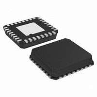
AD7265BCPZ-REEL7 Analog Devices Inc, AD7265BCPZ-REEL7 Datasheet - Page 25

AD7265BCPZ-REEL7
Manufacturer Part Number
AD7265BCPZ-REEL7
Description
IC,Data Acquisition System,3-CHANNEL,12-BIT,LLCC,32PIN,PLASTIC
Manufacturer
Analog Devices Inc
Datasheet
1.AD7265BCPZ-REEL.pdf
(28 pages)
Specifications of AD7265BCPZ-REEL7
Design Resources
AD7265 in Differential and Single-Ended Configurations Using AD8022 (CN0048)
Number Of Bits
12
Sampling Rate (per Second)
1M
Data Interface
DSP, MICROWIRE™, QSPI™, Serial, SPI™
Number Of Converters
2
Power Dissipation (max)
21mW
Voltage Supply Source
Analog and Digital
Operating Temperature
-40°C ~ 125°C
Mounting Type
Surface Mount
Package / Case
32-VFQFN, CSP Exposed Pad
Lead Free Status / RoHS Status
Lead free / RoHS Compliant
For Use With
EVAL-AD7265CB - BOARD EVALUATION FOR AD7265
Lead Free Status / RoHS Status
Lead free / RoHS Compliant
Available stocks
Company
Part Number
Manufacturer
Quantity
Price
Part Number:
AD7265BCPZ-REEL7
Manufacturer:
ADI/亚德诺
Quantity:
20 000
AD7265 TO DSP563xx
The connection diagram in Figure 46 shows how the AD7265
can be connected to the ESSI (synchronous serial interface) of
the DSP563xx family of DSPs from Motorola. There are two
on-board ESSIs, and each operates in synchronous mode
(Bit SYN = 1 in CRB register) with internally generated word
length frame sync for both TX and RX (Bit FSL1 = 0 and
Bit FSL0 = 0 in CRB).
Normal operation of the ESSI is selected by making MOD = 0
in the CRB. Set the word length to 16 by setting Bit WL1 = 1
and Bit WL0 = 0 in CRA.
To implement the power-down modes on the AD7265, the
word length can be changed to 8 bits by setting Bit WL1 = 0 and
Bit WL0 = 0 in CRA. The FSP bit in the CRB should be set to 1
so the frame sync is negative. It is imperative for signal
processing applications that the frame synchronization signal
from the DSP563xx provides equidistant sampling.
Rev. A | Page 25 of 28
In the example shown in Figure 46, the serial clock is taken
from the ESSI0 so the SCK0 pin must be set as an output,
SCKD = 1, while the SCK1 pin is set as an input, SCKD = 0. The
frame sync signal is taken from SC02 on ESSI0, so SCD2 = 1,
while on ESSI1, SCD2 = 0; therefore, SC12 is configured as an
input. The V
voltage as that of the DSP563xx. This allows the ADC to operate
at a higher voltage than its serial interface and therefore the
DSP563xx, if necessary.
1
ADDITIONAL PINS OMITTED FOR CLARITY.
AD7265
Figure 46. Interfacing the AD7265 to the DSP563xx
DRIVE
D
D
V
1
SCLK
OUT
OUT
DRIVE
pin of the AD7265 takes the same supply
CS
A
B
SCK0
SCK1
SRD0
SRD1
SC02
SC12
DSP563xx
V
DD
AD7265
1


