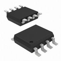
AD7898AR-10REEL7 Analog Devices Inc, AD7898AR-10REEL7 Datasheet - Page 3

AD7898AR-10REEL7
Manufacturer Part Number
AD7898AR-10REEL7
Description
IC,A/D CONVERTER,SINGLE,12-BIT,SOP,8PIN
Manufacturer
Analog Devices Inc
Datasheet
1.AD7898ARZ-10REEL.pdf
(16 pages)
Specifications of AD7898AR-10REEL7
Rohs Status
RoHS non-compliant
Number Of Bits
12
Sampling Rate (per Second)
220k
Data Interface
Serial
Number Of Converters
1
Power Dissipation (max)
22.5mW
Voltage Supply Source
Single Supply
Operating Temperature
-40°C ~ 85°C
Mounting Type
Surface Mount
Package / Case
8-SOIC (0.154", 3.90mm Width)
Lead Free Status / RoHS Status
TIMING SPECIFICATIONS
REV. A
Parameter
Mode 0 Operation
t
t
t
t
t
t
t
t
Mode 1 Operation
f
t
t
t
t
t
t
t
t
t
t
NOTES
1
2
3
4
5
Specifications subject to change without notice.
1
2
3
4
4
5
6
CONVERT
SCLK
CONVERT
QUIET
2
3
4
5
6
7
8
POWER-UP
Sample tested at 25°C to ensure compliance. All input signals are specified with tr = tf = 5 ns (10% to 90% of V
The SCLK maximum frequency is 15 MHz for Mode 0 operation for 220 kSPS throughput with V
The mark/space ratio for SCLK is specified for at least 40% high time (with corresponding 60% low time) or 40% low time (with corresponding 60% high time). As
the SCLK frequency is reduced, the mark/space ratio may vary, provided limits are not exceeded. Care must be taken when interfacing to account for the data access
time, t
See Serial Interface section.
Measured with the load circuit of Figure 1 and defined as the time required for the output to cross 0.8 V or 2.0 V.
t
lated back to remove the effects of charging or discharging the 50 pF capacitor. This means that the time, t
relinquish time of the part and is independent of the bus loading.
Mark/Space ratio for the SCLK input is 40/60 to 60/40.
6
3
3
4
and t
5
4
, and the set-up time required for the users processor. These two times will determine the maximum SCLK frequency that the user’s system can operate with.
8
are derived from the measured time taken by the data outputs to change 0.5 V when loaded with the circuit of Figure 1. The measured number is then extrapo-
Limit at T
40
26
26
30
30
60
70
20
50
3.3
1
3.7
16 × t
4.33
100
70
40
80
108
108
60
20
60
4.33
2
2
2
2
3
3
4
SCLK
MIN
, T
1
MAX
(V
noted.)
DD
= 4.75 V to 5.25 V; V
Unit
ns min
ns min
ns min
ns min
ns min
ns max
ns max
ns min
ns max
µs
kHz min
MHz max
µs max
ns min
ns min
ns max
ns max
ns min
ns min
ns min
ns min
ns max
µs max
Description
CONVST Pulse Width
SCLK High Pulse Width, V
SCLK Low Pulse Width, V
SCLK High Pulse Width V
SCLK Low Pulse Width V
Data Access Time after Falling Edge of SCLK, V
Data Access Time after Falling Edge of SCLK, V
Data Hold Time after Falling Edge of SCLK
Bus Relinquish Time after Falling Edge of SCLK
t
f
Minimum Quiet Time Required between Conversions
CS to SCLK Setup Time
Delay from CS Until SDATA Three-State Disabled
Data Access Time after SCLK Falling Edge
SCLK High Pulse Width
SCLK Low Pulse Width
SCLK to Data Valid Hold Time
SCLK Falling Edge to SDATA High Impedance
SCLK Falling Edge to SDATA High Impedance
Power-Up Time from Power-Down Mode
SCLK
SCLK
DRIVE
–3–
= 1/f
= 3.7 MHz
= 2.7 V to 5.25 V; REF IN = 2.5 V; T
SCLK
DRIVE
= 5 V ± 5%, SCLK = 13 MHz with V
6
and t
DRIVE
DRIVE
DRIVE
DRIVE
DD
8
, quoted in the timing characteristics is the true bus
) and timed from a voltage level of 1.6 V.
= 2.7 V to 3.6 V
= 2.7 V to 3.6 V
= 5 V ± 5%
= 5 V ± 5%
A
= T
MIN
to T
DRIVE
DRIVE
MAX
, unless otherwise
DRIVE
= 5 V ± 5%
= 2.7 V to 3.6 V
AD7898
= 2.7 V to 3.6 V.


