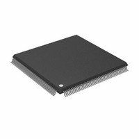
AD8150ASTZ Analog Devices Inc, AD8150ASTZ Datasheet - Page 29

AD8150ASTZ
Manufacturer Part Number
AD8150ASTZ
Description
IC,Telecom Switching Circuit,QFP,184PIN,PLASTIC
Manufacturer
Analog Devices Inc
Datasheet
1.AD8150AST.pdf
(44 pages)
Specifications of AD8150ASTZ
Function
Crosspoint Switch
Circuit
1 x 33:17
Voltage Supply Source
Dual Supply
Voltage - Supply, Single/dual (±)
±3 V ~ 5.5 V
Operating Temperature
0°C ~ 85°C
Mounting Type
Surface Mount
Package / Case
184-LQFP
Lead Free Status / RoHS Status
Lead free / RoHS Compliant
Available stocks
Company
Part Number
Manufacturer
Quantity
Price
Company:
Part Number:
AD8150ASTZ
Manufacturer:
Analog Devices Inc
Quantity:
10 000
APPLICATIONS
AD8150 INPUT AND OUTPUT BUSING
Although the AD8150 is a digital part, in any application that
runs at high speed, analog design details will have to be given
very careful consideration. At high data rates, the design of the
signal channels will have a strong influence on the data integrity
and its associated jitter and ultimately bit error rate (BER).
While it might be considered very helpful to have a suggested
circuit board layout for any particular system configuration, this
is not something that can be practically realized. Systems come
in all shapes, sizes, speeds, performance criteria, and cost
constraints. Therefore, some general design guidelines will be
presented that can be used for all systems and judiciously
modified where appropriate.
High speed signals travel best, that is, maintain their integrity,
when they are carried by a uniform transmission line that is
properly terminated at either end. Any abrupt mismatches in
impedance or improper termination will create reflections that
will add to or subtract from parts of the desired signal. Small
amounts of this effect are unavoidable, but too much will distort
the signal to the point that the channel BER will increase. It is
difficult to fully quantify these effects because they are
influenced by many factors in the overall system design.
A constant-impedance transmission line is characterized by
having a uniform cross-sectional profile over its entire length.
In particular, there should be no stubs, which are branches that
intersect the main run of the transmission line. These can have
an electrical appearance that is approximated by a lumped
element, such as a capacitor, or if long enough, as another
transmission line. To the extent that stubs are unavoidable in a
design, their effect can be minimized by making them as short
as possible and as high an impedance as possible.
Figure 36 shows a differential transmission line that connects
two differential outputs from AD8150s to a generic receiver. A
more generalized system can have more outputs bused and
more receivers on the same bus, but the same concepts apply.
The inputs of the AD8150 can also be considered a receiver.
The transmission lines that bus all of the devices together are
shown with terminations at each end.
Rev. A | Page 29 of 44
The individual outputs of the AD8150 are stubs that intersect
the main transmission line. Ideally, their current-source outputs
would be infinite impedance, and they would have no effect on
signals that propagate along the transmission line. In reality,
each external pin of the AD8150 projects into the package and
has a bond wire connected to the chip inside. On-chip wiring
then connects to the collectors of the output transistors and to
ESD protection diodes.
Unlike some other high speed digital components, the AD8150
does not have on-chip terminations. While the location of such
terminations would be closer to the actual end of the
transmission line for some architectures, this concept can limit
system design options. In particular, it is not possible to bus
more than two inputs or outputs on the same transmission line
and it is not possible to change the value of these terminations
to use them for different impedance transmission lines. The
AD8150, with the added ability to disable its outputs, is much
more versatile in these types of architectures.
If the external traces are kept to a bare minimum, the output
will present a mostly lumped capacitive load of about 2 pF. A
single stub of 2 pF will not seriously adversely affect signal
integrity for most transmission lines, but the more of these
stubs, the more adverse their influence will be.
One way to mitigate this effect is to locally reduce the
capacitance of the main transmission line near the point of stub
intersection. Some practical means for doing this are to narrow
the PC board traces in the region of the stub and/or to remove
some of the ground plane(s) near this intersection. The effect of
these techniques will locally lower the capacitance of the main
transmission line at these points, while the added capacitance of
the AD8150 outputs will compensate for this reduction in
capacitance. The overall intent is to create as uniform a
transmission line as possible.
In selecting the location of the termination resistors, it is
important to keep in mind that, as their name implies, they
should be placed at either end of the line. There should be no,
or minimal, projection of the transmission line beyond the
point where the termination resistors connect to it.
AD8150


