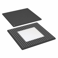
AD8152JBPZ Analog Devices Inc, AD8152JBPZ Datasheet - Page 13

AD8152JBPZ
Manufacturer Part Number
AD8152JBPZ
Description
IC,Telecom Switching Circuit,BGA,256PIN,PLASTIC
Manufacturer
Analog Devices Inc
Datasheet
1.AD8152JBPZ.pdf
(32 pages)
Specifications of AD8152JBPZ
Function
Crosspoint Switch
Circuit
1 x 34:34
Voltage Supply Source
Single Supply
Voltage - Supply, Single/dual (±)
2.5 V ~ 3.3 V
Current - Supply
32mA
Operating Temperature
0°C ~ 85°C
Mounting Type
Surface Mount
Package / Case
256-BGA Exposed Pad, 256-eBGA, 256-HBGA
Lead Free Status / RoHS Status
Lead free / RoHS Compliant
Available stocks
Company
Part Number
Manufacturer
Quantity
Price
Company:
Part Number:
AD8152JBPZ
Manufacturer:
ADI
Quantity:
642
Company:
Part Number:
AD8152JBPZ
Manufacturer:
Analog Devices Inc
Quantity:
10 000
Connection/Current Bit
A6
0 = CONNECTION LATCHES
1 = OUTPUT CURRENT LEVEL
Connection/
Current Bit
0 = CONNECTION
A6
0
0
0
0
0
0
0
Connection/
Current Bit
1 = CURRENT LEVEL MSB
A6
1
1
1
1
RESET CS
0
1
1
1
1
1
REV. A
X
1
0
0
0
0
WE
X
X
0
X
X
0
RE
X
X
1
0
X
1
Output Address Pins
A5 A4 A3 A2 A1 A0
0
0
1
1
Table III. Output-Current Level Data and Address Programming Examples
Output Address Pins
MSB
A5 A4 A3 A2 A1 A0
0
0
1
1
0
1
1
0
0
0
1
UPD Function
X
X
X
X
0
0
0
0
0
1
0
0
1
Table II. Connection Data and Address Programming Examples
0
0
0
1
0
0
0
1
0
0
1
Global Reset. Disables all outputs and resets all output current to code 0111 (16 mA).
Disable All Control Signals. Signal matrix/currents remain the same. D5:D0 are high impedance.
Write Enable. Write D5:D0 data into first rank register addressed by A6:A0.
Single-Output Readback. Second rank register data for output A6:A0 appears on D5:D0.
Global Update. Copy all first rank data into second rank registers.
Transparent Write and Update. D5:D0 immediately control programming. Use RE as gating signal.
0
0
0
1
0
0
0
1
0
0
1
Output Address Pins
A5
MSB
0
0
0
1
Table IV. Basic Control Strobe Functions
0
0
0
1
0
0
1
A4
Table I. Address and Data Buses
LSB MSB
0
0
1
1
LSB
0
0
1
1
0
1
1
A3
Data Pins
(Used to Select Inputs)
D5
X
X
X
X
Data Pins
(Used to Select Inputs)
MSB
D5 D4 D3 D2 D1 D0
0
1
0
0
1
1
1
D4 D3 D2 D1 D0
X
X
X
X
A2
–13–
0
0
1
0
1
1
1
0
1
0
1
0
0
1
0
1
1
1
A1
0
1
1
0
0
0
1
0
1
1
1
A0
LSB
0
1
1
0
0
0
1
0
1
1
1
LSB
0
1
1
0
LSB
0
1
1
0
1
1
1
Data Pins
D5
Program OUT00 to Current—Code 00 (2 mA)
Program OUT00 to Current—Code 15 (32 mA)
Program OUT33 to Current—Code 07 (16 mA)
Broadcast Current—Code 08 to All
Outputs (18 mA)
MSB
Comments
Comments
Program IN00 to OUT00
Program IN33 to OUT00
Program IN31 to OUT33
Broadcast IN00 to All Outputs
Disable OUT00
Disable OUT33
Disable All Outputs (Broadcast)
D4
D3
D2
D1
AD8152
D0
LSB


