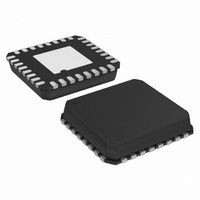
AD8193ACPZ Analog Devices Inc, AD8193ACPZ Datasheet

AD8193ACPZ
Specifications of AD8193ACPZ
Related parts for AD8193ACPZ
AD8193ACPZ Summary of contents
Page 1
FEATURES 2 inputs, 1 output HDMI/DVI high speed signal switch Pin-to-pin compatible with the AD8194 Enables HDMI 1.3-compliant receiver 4 TMDS channels per input/output Supports 250 Mbps to 2.25 Gbps data rates Supports 25 MHz to 225 MHz pixel clocks ...
Page 2
AD8193 TABLE OF CONTENTS Features .............................................................................................. 1 Applications....................................................................................... 1 Functional Block Diagram .............................................................. 1 Typical Application........................................................................... 1 General Description ......................................................................... 1 Product Highlights ........................................................................... 1 Revision History ............................................................................... 2 Specifications..................................................................................... 3 Absolute Maximum Ratings............................................................ 4 Thermal Resistance ...................................................................... 4 Maximum ...
Page 3
SPECIFICATIONS T = 27°C, AVCC = 3.3 V, VTTI = 3.3 V, VTTO = 3.3 V, AVEE = 0 V, differential input swing = 1000 mV, pattern = PRBS 2 A data rate = 2.25 Gbps, TMDS outputs terminated with ...
Page 4
AD8193 ABSOLUTE MAXIMUM RATINGS Table 2. Parameter Rating AVCC to AVEE 3.7 V VTTI AVCC + 0.6 V VTTO AVCC + 0.6 V Internal Power Dissipation 1.2 W High Speed Input Voltage AVCC − 1.4 V < V High Speed ...
Page 5
PIN CONFIGURATION AND FUNCTION DESCRIPTIONS NOTES 1. THE AD8193 LFCSP HAS AN EXPOSED PADDLE (ePAD) ON THE UNDERSIDE OF THE PACKAGE, WHICH AIDS IN HEAT DISSIPATION. THE ePAD MUST BE ELECTRICALLY CONNECTED TO THE AVEE SUPPLY PLANE TO MEET THERMAL ...
Page 6
AD8193 TYPICAL PERFORMANCE CHARACTERISTICS T = 27°C, AVCC = 3.3 V, VTTI = 3.3 V, VTTO = 3.3 V, AVEE = 0 V, differential input swing = 1000 mV, pattern = PRBS 2 A data rate = 2.25 Gbps, TMDS ...
Page 7
T = 27°C, AVCC = 3.3 V, VTTI = 3.3 V, VTTO = 3.3 V, AVEE = 0 V, differential input swing = 1000 mV, pattern = PRBS 2 A data rate = 2.25 Gbps, TMDS outputs terminated with external ...
Page 8
AD8193 T = 27°C, AVCC = 3.3 V, VTTI = 3.3 V, VTTO = 3.3 V, AVEE = 0 V, differential input swing = 1000 mV, pattern = PRBS 2 A data rate = 2.25 Gbps, TMDS outputs terminated with ...
Page 9
THEORY OF OPERATION INTRODUCTION The primary function of the AD8193 is to switch the high speed signals from one of two (HDMI or DVI) single-link sources to one output. Each source group consists of four differential, high speed channels. The ...
Page 10
AD8193 OUTPUT CHANNELS Each high speed output differential pair is terminated to the 3.3 V VTTO power supply through two single-ended 50 Ω on-chip resistors, as shown in Figure 20. These matched on- chip back-terminations absorb reflections on the output ...
Page 11
APPLICATION NOTES SWITCHING HIGH SPEED SIGNALS The AD8193 is a quad 2:1 TMDS switch that is used to switch the high speed signals of two input HDMI links to a single HDMI output. SWITCHING LOW SPEED SIGNALS Because the AD8193 ...
Page 12
AD8193 Both traces of a given differential pair must be equal in length to minimize intrapair skew. Maintaining the physical symmetry of a differential pair is integral to ensuring its signal integrity; excessive intrapair skew can introduce jitter through duty ...
Page 13
Auxiliary Control Signals There are four single-ended control signals associated with each source or sink in an HDMI/DVI application. These are hot plug detect (HPD), consumer electronics control (CEC), and two display data channel (DDC) lines. The two signals on ...
Page 14
AD8193 Evaluation Board The AD8193 evaluation board illustrates one way to implement a 2:1 HDMI link switch with an AD8193 and a CMOS switch. The AD8193 evaluation board deviates from a typical applica- tion in that it uses an HDMI ...
Page 15
Figure 26 shows the layout of the TMDS traces. These are 100 Ω differential, controlled-impedance traces. Serpentine traces are used for some of the paths to match the lengths within a group of four. The gray traces are routed on ...
Page 16
... BE BENEFICIAL IN HIGH TEMPERATURE ENVIRONMENTS. ORDERING GUIDE Temperature Model Range 1 AD8193ACPZ −40°C to +85°C 1 AD8193ACPZ-R7 −40°C to +85°C 1 AD8193-EVALZ RoHS Compliant Part. ©2007 Analog Devices, Inc. All rights reserved. Trademarks and registered trademarks are the property of their respective owners. D07003-0-11/07(0) 5 ...


