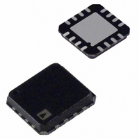
AD8222BCPZ-RL Analog Devices Inc, AD8222BCPZ-RL Datasheet - Page 19

AD8222BCPZ-RL
Manufacturer Part Number
AD8222BCPZ-RL
Description
IC,Instrumentation Amplifier,DUAL,LLCC,16PIN,PLASTIC
Manufacturer
Analog Devices Inc
Datasheet
1.AD8222BCPZ-R7.pdf
(24 pages)
Specifications of AD8222BCPZ-RL
Amplifier Type
Instrumentation
Number Of Circuits
2
Slew Rate
2 V/µs
-3db Bandwidth
1.2MHz
Current - Input Bias
200pA
Voltage - Input Offset
60µV
Current - Supply
900µA
Current - Output / Channel
18mA
Voltage - Supply, Single/dual (±)
4.6 V ~ 36 V, ±2.3 V ~ 18 V
Operating Temperature
-40°C ~ 85°C
Mounting Type
Surface Mount
Package / Case
16-LFCSP
Lead Free Status / RoHS Status
Lead free / RoHS Compliant
Output Type
-
Gain Bandwidth Product
-
Lead Free Status / RoHS Status
Lead free / RoHS Compliant
APPLICATIONS INFORMATION
DIFFERENTIAL OUTPUT
The differential configuration of the AD8222 has the same
excellent dc precision specifications as the single-ended output
configuration and is recommended for applications in the
frequency range of dc to 100 kHz.
The circuit configuration is shown in Figure 49. The differential
output specifications in Table 2 and Table 4 refer to this configura-
tion only. The circuit includes an RC filter that maintains the
stability of the loop.
The transfer function for the differential output is:
where
V
DIFF_OUT
G
1
+IN
–IN
R
G
= V
49.4
Figure 49. Differential Circuit Schematic
+OUT
R
AD8222
+
–
G
kΩ
− V
−OUT
AD8222
REF2
= (V
+IN
+
–
− V
10kΩ
−IN
100pF
) × G
+OUT
+IN2
–OUT
Rev. A | Page 19 of 24
Setting the Common-Mode Voltage
The output common-mode voltage is set by the average of +IN2
and REF2. The transfer function is
+IN2 and REF2 have different properties that allow the
reference voltage to be easily set for a wide variety of applications.
+IN2 has high impedance but cannot swing to the supply rails
of the part. REF2 must be driven with a low impedance but can
go 300 mV beyond the supply rails.
A common application sets the common-mode output voltage
to the midscale of a differential ADC. In this case, the ADC
reference voltage is sent to the +IN2 terminal, and ground is
connected to the REF2 terminal. This produces a common-mode
output voltage of half the ADC reference voltage.
2-Channel Differential Output Using a Dual Op Amp
Another differential output topology is shown in Figure 50.
Instead of a second in-amp, ½ of a dual OP2177 op amp creates
the inverted output. Because the
MSOP, this configuration allows the creation of a dual channel,
precision differential output in-amp with little board area.
Errors from the op amp are common to both outputs and are
thus common mode. Errors from mismatched resistors also
create a common-mode dc offset. Because these errors are
common mode, they will likely be rejected by the next device
in the signal chain.
V
CM_OUT
+IN
–IN
= (V
Figure 50. Differential Output Using Op Amp
AD8222
+OUT
REF
+ V
4.99kΩ
4.99kΩ
−OUT
)/2 = (V
OP2177
–
OP2177
+IN2
+ V
is packaged in an
V
REF
+
REF2
+OUT
–OUT
)/2
AD8222


