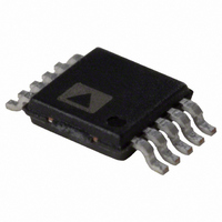
AD8271ARMZ-R7 Analog Devices Inc, AD8271ARMZ-R7 Datasheet - Page 15

AD8271ARMZ-R7
Manufacturer Part Number
AD8271ARMZ-R7
Description
High BW, G = 0.5, 1, 2, 3
Manufacturer
Analog Devices Inc
Datasheet
1.AD8271ARMZ-R7.pdf
(20 pages)
Specifications of AD8271ARMZ-R7
Design Resources
High Speed Instrumentation Amplifier Using AD8271 and ADA4627-1 (CN0122)
Amplifier Type
Programmable Gain
Number Of Circuits
1
Output Type
Rail-to-Rail
Slew Rate
30 V/µs
Gain Bandwidth Product
15MHz
Current - Input Bias
500nA
Voltage - Input Offset
300µV
Current - Supply
2.3mA
Current - Output / Channel
100mA
Voltage - Supply, Single/dual (±)
5 V ~ 36 V, ±2.5 V ~ 18 V
Operating Temperature
-40°C ~ 85°C
Mounting Type
Surface Mount
Package / Case
10-MSOP, Micro10™, 10-uMAX, 10-uSOP
Lead Free Status / RoHS Status
Lead free / RoHS Compliant
-3db Bandwidth
-
Lead Free Status / RoHS Status
Lead free / RoHS Compliant
Other names
AD8271ARMZ-R7TR
Available stocks
Company
Part Number
Manufacturer
Quantity
Price
Company:
Part Number:
AD8271ARMZ-R7
Manufacturer:
MICREL
Quantity:
4 379
THEORY OF OPERATION
CIRCUIT INFORMATION
The AD8271 consists of a high precision, low distortion op amp
and seven trimmed resistors. These resistors can be connected
to create a wide variety of amplifier configurations, including
difference, noninverting, and inverting configurations. The
resistors on the chip can be connected in parallel for a wider range
of options. Using the on-chip resistors of the AD8271 provides
the designer with several advantages over a discrete design.
DC Performance
Much of the dc performance of op amp circuits depends on the
accuracy of the surrounding resistors. The resistors on the AD8271
are laid out to be tightly matched. The resistors of each part are
laser trimmed and tested for their matching accuracy. Because
of this trimming and testing, the AD8271 can guarantee high
accuracy for specifications, such as gain drift, common-mode
rejection, and gain error.
AC Performance
Because feature size is much smaller in an integrated circuit than
on a printed circuit board (PCB), the corresponding parasitics are
also smaller. The smaller feature size helps the ac performance of
the AD8271. For example, the positive and negative input terminals
of the AD8271 op amp are not pinned out intentionally. By not
connecting these nodes to the traces on the PCB, the capacitance
remains low, resulting in both improved loop stability and
common-mode rejection over frequency.
Production Costs
Because one part, rather than several discrete components, is
placed on the PCB, the board can be built more quickly and
efficiently.
Size
The AD8271 fits an op amp and seven resistors in one MSOP
package.
DRIVING THE AD8271
The AD8271 is easy to drive, with all configurations presenting
at least several kilohms (kΩ) of input resistance. The AD8271
should be driven with a low impedance source: for example,
another amplifier. The gain accuracy and common-mode rejection
–V
P1
P2
P3
P4
S
Figure 43. Functional Block Diagram
1
2
3
4
5
10kΩ
10kΩ
20kΩ
20kΩ
AD8271
10kΩ
10kΩ
10kΩ
10
9
8
7
6
+V
N3
N2
N1
OUT
S
Rev. 0 | Page 15 of 20
of the AD8271 depend on the matching of its resistors. Even
source resistance of a few ohms can have a substantial effect on
these specifications.
POWER SUPPLIES
A stable dc voltage should be used to power the AD8271. Noise
on the supply pins can adversely affect performance. A bypass
capacitor of 0.1 μF should be placed between each supply pin
and ground, as close as possible to each supply pin. A tantalum
capacitor of 10 μF should also be used between each supply and
ground. It can be farther away from the supply pins and, typically,
it can be shared by other precision integrated circuits.
The AD8271 is specified at ±15 V and ±5 V, but it can be used with
unbalanced supplies, as well. For example, −V
The difference between the two supplies must be kept below 36 V.
INPUT VOLTAGE RANGE
The AD8271 has a true rail-to-rail input range for the majority
of applications. Because most AD8271 configurations divide down
the voltage before they reach the internal op amp, the op amp sees
only a fraction of the input voltage. Figure 44 shows an example
of how the voltage division works in the difference amplifier
configuration.
The internal op amp voltage range may be relevant in the
following applications, and calculating the voltage at the
internal op amp is advised.
•
•
•
For correct operation, the input voltages at the internal op amp
must stay within 1.5 V of either supply rail.
Voltages beyond the supply rails should not be applied to the
part. The part contains ESD diodes at the input pins, which
conduct if voltages beyond the rails are applied. Currents greater
than 5 mA may damage these diodes and the part. For a similar
part that can operate with voltages beyond the rails, see the
AD8274
Figure 44. Voltage Division in the Difference Amplifier Configuration
Difference amplifier configurations using supply voltages
of less than ±4.5 V
Difference amplifier configurations with a reference
voltage near the rail
Single-ended amplifier configurations
data sheet.
R1 + R2
R2
R3
R1
(V
R2
+IN
)
R1 + R2
R2
R4
(V
+IN
)
S
= 0 V, +V
AD8271
S
= 20 V.


