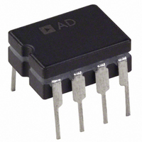
AD847SQ Analog Devices Inc, AD847SQ Datasheet - Page 12

AD847SQ
Manufacturer Part Number
AD847SQ
Description
Amplifier IC
Manufacturer
Analog Devices Inc
Type
General Purpose Amplifierr
Datasheet
1.AD847JNZ.pdf
(12 pages)
Specifications of AD847SQ
Mounting Type
Through Hole
Package / Case
8-CDIP
Rohs Status
RoHS non-compliant
Amplifier Type
General Purpose
Number Of Circuits
1
Slew Rate
300 V/µs
Gain Bandwidth Product
50MHz
Current - Input Bias
3.3µA
Voltage - Input Offset
500µV
Current - Supply
5.3mA
Current - Output / Channel
32mA
Voltage - Supply, Single/dual (±)
±4.5 V ~ 18 V
Operating Temperature
-55°C ~ 125°C
Rail/rail I/o Type
No
Number Of Elements
1
Unity Gain Bandwidth Product
35MHz
Common Mode Rejection Ratio
80dB
Input Offset Voltage
1mV
Input Bias Current
5uA
Single Supply Voltage (typ)
Not RequiredV
Dual Supply Voltage (typ)
±5/±9/±12/±15V
Power Dissipation
1.1W
Voltage Gain In Db
70.88dB
Power Supply Rejection Ratio
75dB
Power Supply Requirement
Dual
Shut Down Feature
No
Single Supply Voltage (min)
Not RequiredV
Single Supply Voltage (max)
Not RequiredV
Dual Supply Voltage (min)
±4.5V
Dual Supply Voltage (max)
±18V
Technology
BiCOM
Operating Temp Range
-55C to 125C
Operating Temperature Classification
Military
Mounting
Through Hole
Pin Count
8
Package Type
CDIP
Output Type
-
-3db Bandwidth
-
Lead Free Status / Rohs Status
Not Compliant
Available stocks
Company
Part Number
Manufacturer
Quantity
Price
Part Number:
AD847SQ
Manufacturer:
ADI/亚德诺
Quantity:
20 000
Part Number:
AD847SQ/883B
Manufacturer:
ADI/亚德诺
Quantity:
20 000
Company:
Part Number:
AD847SQ883B
Manufacturer:
INTEL
Quantity:
15
All brand or product names mentioned are trademarks or registered trademarks of their respective holders.
AD847
HIGH SPEED DAC BUFFER
The wide bandwidth and fast settling time of the AD847 makes
it a very good output buffer for high speed current-output D/A
converters like the AD668. As shown in Figure 27, the op amp
establishes a summing node at ground for the DAC output. The
output voltage is determined by the amplifier’s feedback resistor
(4.19±0.25)
0.165±0.01
(3.18)
0.125
PIN 1
MIN
0.018±0.003
(0.46±0.08)
Mini-DIP (N-8) Package
8
1
0.39 (9.91) MAX
0.011±0.003
0.30 (7.62)
15
(0.28±0.08)
0
(2.54)
°
0.10
BSC
°
REF
0.033
(0.84)
NOM
4
5
0.035±0.01
(0.89±0.25)
(6.35)
0.25
SEATING
PLANE
0.18±0.03
(4.57±0.76)
(7.87)
0.31
DIGITAL
INPUTS
10
11
12
1
2
4
5
9
3
6
7
8
MSB
LSB
AD668
Figure 27. High Speed DAC Buffer
Dimensions shown in inches and (mm).
0.200 (5.08)
0.125 (3.18)
REFCOM
REFIN2
THCOM
REFIN1
R
ACOM
LCOM
OUTLINE DIMENSIONS
(5.08)
0.200
IBPO
MAX
LOAD
I
0.005 (0.13) MIN
PIN 1
VTH
V
OUT
V
Cerdip (Q-8) Package
CC
EE
0.023 (0.58)
0.014 (0.36)
23
20
22
21
19
18
17
16
15
14
13
24
8
1
0.405 (10.29) MAX
+15V
0.320 (8.13)
0.290 (7.37)
15
0.015 (0.38)
0.008 (0.20)
0
0.100
(2.54)
BSC
–12–
100pF
0.1 F
10 F
ANALOG GROUND PLANE
0.055 (1.40) MAX
0.070 (1.78)
0.030 (0.76)
(10.24 V for a 1 k resistor). Note that since the DAC gener-
ates a positive current to ground, the voltage at the amplifier
output will be negative. A 100
noninverting amplifier input and ground minimizes the offset
effects of op amp input bias currents.
0.1 F
100
1k
4
5
10k
0.310 (7.87)
0.220 (5.59)
0.060 (1.52)
0.015 (0.38)
TO ANALOG
GROUND PLANE
SEATING
PLANE
10 F
0.150
(3.81)
MIN
AD847
+5V
–15V
+
–
1k
1V NOMINAL
REFERENCE INPUT
ANALOG
SUPPLY
GROUND
ANALOG
OUTPUT
0.098 (0.2482)
0.075 (0.1905)
Small Outline (R-8) Package
0.010 (0.25)
0.004 (0.10)
0.244 (6.20)
0.228 (5.79)
0.020 (0.051) x 45
CHAMF
PIN 1
8
0
series resistor between the
°
°
1
0.050
(1.27)
8
BSC
10
0
0.197 (5.01)
0.189 (4.80)
0.150 (3.81)
0.190 (4.82)
0.170 (4.32)
°
°
°
0.019 (0.48)
0.014 (0.36)
4
5
0.030 (0.76)
0.018 (0.46)
0.102 (2.59)
0.094 (2.39)
0.157 (3.99)
0.150 (3.81)
0.090
(2.29)
REV. F


