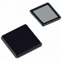
AD9601BCPZ-200 Analog Devices Inc, AD9601BCPZ-200 Datasheet - Page 19

AD9601BCPZ-200
Manufacturer Part Number
AD9601BCPZ-200
Description
IC,A/D CONVERTER,SINGLE,10-BIT,CMOS,LLCC,56PIN
Manufacturer
Analog Devices Inc
Datasheet
1.AD9601BCPZ-200.pdf
(32 pages)
Specifications of AD9601BCPZ-200
Number Of Bits
10
Sampling Rate (per Second)
200M
Data Interface
Serial, SPI™
Number Of Converters
1
Power Dissipation (max)
291mW
Voltage Supply Source
Single Supply
Operating Temperature
-40°C ~ 85°C
Mounting Type
Surface Mount
Package / Case
56-LFCSP
Lead Free Status / RoHS Status
Lead free / RoHS Compliant
For Use With
AD9601-250EBZ - BOARD EVALUATION AD9601-250
Lead Free Status / RoHS Status
Lead free / RoHS Compliant
TIMING—SINGLE PORT MODE
In single port mode, the CMOS output data is available from
Data Port A (DA0 to DA9). The outputs for Port B (DB0 to
DB9) are unused, and are high impedance in this mode.
The Port A outputs and the differential output data clock
(DCO+/DCO−) switch nearly simultaneously during the rising
edge of DCO+. In this mode, it is recommended to use the
rising edge of DCO− to capture the data from Port A. The setup
and hold time depends on the input sample clock period, and is
approximately 1/f
TIMING—INTERLEAVED MODE
In interleaved mode, the output data of the AD9601 is de-
multiplexed onto two data port buses, Port A (DA0 to DA9) and
Port B (DB0 to DB9). The output data and differential data
capture clock switch at one-half the rate of the sample clock
input (CLK+/CLK−), increasing the setup and hold time for the
external data capture circuit relative to single port mode (see
Figure 3, interleaved mode timing diagram). The two ports
switch on alternating sample clock cycles, with the data for
Port A being valid during the rising edge of DCO+, and the
data for Port B being valid during the rising edge of DCO−. The
pipeline latency for both ports is six sample clock cycles. Due to
the random nature of the ÷2 circuit that generates the timing
for the output stage in interleaved mode, the first data sample
during power-up can be assigned to either Data Port A or Port
B. The user cannot control the polarity of the output data clock
relative to the input sample clock. In this mode, it is recom-
CLK
± t
SKEW
.
Rev. 0 | Page 19 of 32
mended to use the rising edge of DCO+ to capture the data
from Port A, and the rising edge of DCO− to capture the data
from Port B. In both cases, the setup and hold time depends on
the input sample clock period, and both are approximately
2/f
f
Because the AD9601 output data rate is at one-half the sampling
frequency in interleaved output mode, there is significant f
energy in the outputs of the part, and there is significant energy
in the ADC output spectrum at f
certain that this f
circuit or the analog inputs of the AD9601. When f
coupled in this fashion, it appears as a spurious tone reflected
around f
sampling application with a 90 MHz single-tone analog input,
this energy generates a tone at 97.5 MHz.
Depending on the relationship of the IF frequency to the center
of the Nyquist zone, this spurious tone may or may not be in the
user’s band of interest. Some residual f
the AD9601, and the level of this spur is typically below the
level of the harmonics at clock rates. Figure 20 shows a plot of
the f
AD9601-250. For the specifications provided in Table 2, the f
spur effect is not a factor, as the device is specified in single port
output mode.
S
/2 Spurious
S
± t
S
[(3 × 125 MSPS/4 − 90 MHz) + 3 × 125 MSPS/4]
/2 spur level vs. the analog input frequency for the
SKEW
S
/4, 3f
.
S
/4, 5f
S
/2 energy does not couple into either the clock
S
/4, and so on. For example, in a 125 MSPS
S
/2. Care must be taken to be
S
/2 energy is present in
S
/2 energy is
AD9601
S
/2
S
/2


