AD9776BSVZ Analog Devices Inc, AD9776BSVZ Datasheet - Page 46
AD9776BSVZ
Manufacturer Part Number
AD9776BSVZ
Description
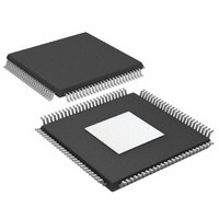
IC,D/A CONVERTER,DUAL,12-BIT,CMOS,TQFP,100PIN
Manufacturer
Analog Devices Inc
Datasheet
1.AD9776BSVZRL.pdf
(56 pages)
Specifications of AD9776BSVZ
Number Of Bits
12
Data Interface
Parallel
Number Of Converters
2
Voltage Supply Source
Analog and Digital
Power Dissipation (max)
300mW
Operating Temperature
-40°C ~ 85°C
Mounting Type
Surface Mount
Package / Case
100-TQFP Exposed Pad, 100-eTQFP, 100-HTQFP, 100-VQFP
Lead Free Status / RoHS Status
Lead free / RoHS Compliant
For Use With
AD9776A-EBZ - BOARD EVALUATION AD9776A
Settling Time
-
Lead Free Status / RoHS Status
Lead free / RoHS Compliant
Available stocks
Company
Part Number
Manufacturer
Quantity
Price
Company:

Part Number:
AD9776BSVZ
Manufacturer:
Analog Devices Inc
Quantity:
10 000
Company:
Part Number:
AD9776BSVZRL
Manufacturer:
Analog Devices Inc
Quantity:
10 000


AD9776/AD9778/AD9779
EVALUATION BOARD OPERATION
The AD977x evaluation board is designed to optimize the DAC
performance and the speed of the digital interface, yet remains
user friendly. To operate the board, the user needs a power
source, a clock source, and a digital data source. The user also
needs a spectrum analyzer or an oscilloscope to look at the DAC
output. The diagram in Figure 100 illustrates the test setup. A
sine or square wave clock works well as a clock source. The dc
offset on the clock is not a problem, since the clock is ac-coupled
on the evaluation board before the REFCLK inputs. All
necessary connections to the evaluation board are shown in
more detail in Figure 101.
CLOCK IN
GENERATOR
PATTERN
DIGITAL
P4 Digital Input Connector
DATACLK OUT
Figure 101. AD977x Evaluation Board Showing All Connections
ADAPTER
AUX33
CABLES
S7 DCLKOUT
GENERATOR
DVDD18
CLOCK
Figure 100. Typical Test Setup
CLKIN
Rev. A | Page 46 of 56
AD9779
EVALUATION
SPI PORT
AD9779
DVDD33
BOARD
SPI PORT
J1 CLOCK IN
JP15
JP14
JP16
JP17
JP4
JP8
JP3
JP2
CVDD18
The evaluation board comes with software that allows the user
to program the SPI port. Via the SPI port, the devices can be
programmed into any of its various operating modes. When
first operating the evaluation board, it is useful to start with a
simple configuration, that is, a configuration in which the SPI
port settings are as close as possible to the default settings. The
default software window is shown in Figure 102. The arrows
indicate which settings need to be changed for an easy first time
evaluation. Note that this implies that the PLL is not being used
and that the clock being used is at the speed of the DAC output
sample rate. For a more detailed description of how to use the
PLL, see the PLL Loop Filter Bandwidth section.
S5 OUTPUT 1
S6 OUTPUT 2
AVDD33
AD8349
1.8V POWER SUPPLY
3.3V POWER SUPPLY
MODULATOR
AD9779/8/6
SPECTRUM
ANALYZER
ANALOG
DEVICES
LOCAL OSC
OUTPUT
REV D
5V Supply
INPUT
J2
+5V
GND
Related parts for AD9776BSVZ
Image
Part Number
Description
Manufacturer
Datasheet
Request
R

Part Number:
Description:
BOARD EVALUATION FOR AD9776
Manufacturer:
Analog Devices Inc
Datasheet:
Part Number:
Description:
BOARD EVALUATION FOR AD9776
Manufacturer:
Analog Devices Inc
Datasheet:

Part Number:
Description:
±1.7g Dual-Axis IMEMS Accelerometer Evaluation Board
Manufacturer:
Analog Devices Inc
Datasheet:
Part Number:
Description:
Inertial Sensor Evaluation System
Manufacturer:
Analog Devices Inc
Datasheet:
Part Number:
Description:
Manufacturer:
Analog Devices Inc
Datasheet:
Part Number:
Description:
Manufacturer:
Analog Devices Inc
Datasheet:
Part Number:
Description:
Manufacturer:
Analog Devices Inc
Datasheet:
Part Number:
Description:
Manufacturer:
Analog Devices Inc
Datasheet:
Part Number:
Description:
Manufacturer:
Analog Devices Inc
Datasheet:
Part Number:
Description:
Manufacturer:
Analog Devices Inc
Datasheet:
Part Number:
Description:
Manufacturer:
Analog Devices Inc
Datasheet:
Part Number:
Description:
Manufacturer:
Analog Devices Inc
Datasheet:
Part Number:
Description:
Manufacturer:
Analog Devices Inc
Datasheet: