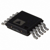
ADA4310-1ARHZ-RL Analog Devices Inc, ADA4310-1ARHZ-RL Datasheet

ADA4310-1ARHZ-RL
Specifications of ADA4310-1ARHZ-RL
Related parts for ADA4310-1ARHZ-RL
ADA4310-1ARHZ-RL Summary of contents
Page 1
... The CMOS- compatible, power-down control pins (PD1 and PD0) enable the ADA4310-1 to operate in four different modes: full power, medium power, low power, and complete power down. In the power-down mode, quiescent current drops to only ...
Page 2
... ADA4310-1 TABLE OF CONTENTS Features .............................................................................................. 1 Applications....................................................................................... 1 Pin Configurations ........................................................................... 1 General Description ......................................................................... 1 Revision History ............................................................................... 2 Specifications..................................................................................... 3 Absolute Maximum Ratings............................................................ 5 Thermal Resistance ...................................................................... 5 ESD Caution.................................................................................. 5 Pin Configurations and Function Descriptions ........................... 6 Typical Performance Characteristics ............................................. 7 REVISION HISTORY 10/06—Revision 0: Initial Version Theory of Operation ...................................................................... 10 Application Information................................................................ 11 Feedback Resistor Selection...................................................... 11 Power Control Modes of Operation ........................................ 11 Exposed Thermal Pad Connections ...
Page 3
... LOAD Ω LOAD R = 100 Ω LOAD R = 100 Ω LOAD R = 100 Ω LOAD PD1 = 0, PD0 = 0 PD1 = 0, PD0 = 1 PD1 = 1, PD0 = 0 PD1 = 1, PD0 = 1 Rev Page ADA4310-1 Min Typ Max Unit 190 MHz 140 MHz 100 MHz 820 V/μs 790 V/μs 750 V/μs −95 dBc − ...
Page 4
... ADA4310-1 Parameter POWER DOWN PINS PD1, PD0 Threshold PD1, PD0 = 0 Pin Bias Current PD1, PD0 = 1 Pin Bias Current Enable/Disable Time Power Supply Rejection Ratio Test Conditions/Comments Referenced to GND PD1 or PD0 = 0 V PD1 or PD0 = 3 V Positive/Negative Rev Page Min Typ Max Unit 1 ...
Page 5
... Therefore, proper ESD precautions are recommended to avoid performance degradation or loss of functionality. Maximum Power Dissipation Rating The maximum safe power dissipation for the ADA4310-1 is limited by the associated rise in junction temperature ( the die. At approximately 150°C, which is the glass transition ±6V temperature, the plastic changes its properties ...
Page 6
... ADA4310-1 PIN CONFIGURATIONS AND FUNCTION DESCRIPTIONS + OUT – + CONNECT Figure 5. 10-Lead MSOP Pin Configuration Table 4. 10-Lead MSOP Pin Function Description Pin No. Mnemonic Description 1 +V Positive Power Supply Input Connection 3 OUT A Amplifier A Output 4 −IN A Amplifier A Inverting Input 5 +IN A Amplifier A Noninverting Input 6 PD0 ...
Page 7
... FREQUENCY (MHz) Figure 10. Harmonic Distortion vs. Frequency 100 100 1k 10k 100k 1M 10M FREQUENCY (Hz) Figure 11. Voltage Noise vs. Frequency 0. 50Ω L 0.15 10ns/DIV 0.10 0.05 0 –0.05 –0.10 –0.15 –0.20 Figure 12. Small Signal Transient Response ADA4310-1 HD2 HD3 100 100M 1G ...
Page 8
... ADA4310-1 0 PD1, PD0 = ( 100Ω L –10 –20 –30 –40 –50 –60 –70 0.01 0 FREQUENCY (MHz) Figure 13. Common-Mode Rejection(CMR) vs. Frequency PD1, PD0 = (0, 0) – 100Ω L –20 –30 +PSR –40 –PSR –50 –60 –70 –80 0.01 0 FREQUENCY (MHz) Figure 14. Power Supply Rejection(PSR) vs. Frequency ...
Page 9
... FREQUENCY (MHz) Figure 19. Crosstalk 1000 Rev Page ADA4310-1 ...
Page 10
... ADA4310-1 THEORY OF OPERATION The ADA4310 current feedback amplifier with high output current capability. With a current feedback amplifier, the current into the inverting input is the feedback signal, and the open-loop behavior is that of a transimpedance, dV The open-loop transimpedance is analogous to the open-loop voltage gain of a voltage feedback amplifier. Figure 20 shows a simplified model of a current feedback amplifier ...
Page 11
... PD pins and the only electrical connection for the negative supply voltage. Therefore, in the 10-lead MSOP package, the ADA4310-1 can only be used on a single supply. The exposed thermal pad MUST be connected to ground. Failure will render the part inoperable. ...
Page 12
... A Practical Guide to High-Speed Printed- Circuit-Board Layout. POWER SUPPLY BYPASSING The ADA4310-1 operates on supplies, from + ±6 V. The ADA4310-1 circuit should be powered with a well-regulated power supply. Careful attention must be paid to decoupling the power supply. High quality capacitors with low equivalent series ...
Page 13
... Figure 22. 10-Lead Mini Small Outline Package with Exposed Pad [MINI_SO_EP] PIN 1 INDICATOR 12° MAX 1.00 0.85 0.80 ORDERING GUIDE Temperature Model Package ADA4310-1ARHZ-RL 1 −40°C to +85°C 1 ADA4310-1ARHZ-R7 −40°C to +85°C ADA4310-1ARHZ 1 −40°C to +85°C 1 ADA4310-1ACPZ-RL −40°C to +85°C ...
Page 14
... ADA4310-1 NOTES Rev Page ...
Page 15
... NOTES Rev Page ADA4310-1 ...
Page 16
... ADA4310-1 NOTES ©2006 Analog Devices, Inc. All rights reserved. Trademarks and registered trademarks are the property of their respective owners. D06027-0-10/06(0) Rev Page ...


