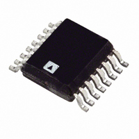
ADA4420-6ARQZ Analog Devices Inc, ADA4420-6ARQZ Datasheet - Page 4

ADA4420-6ARQZ
Manufacturer Part Number
ADA4420-6ARQZ
Description
Intrgratd VID Fltr & Buf For HD&SD Video
Manufacturer
Analog Devices Inc
Type
Video Filterr
Datasheet
1.ADA4420-6ARQZ.pdf
(12 pages)
Specifications of ADA4420-6ARQZ
Applications
DVD, HD, Set-Top Boxes, Recorders
Mounting Type
Surface Mount
Package / Case
16-QSOP
Lead Free Status / RoHS Status
Lead free / RoHS Compliant
Available stocks
Company
Part Number
Manufacturer
Quantity
Price
Company:
Part Number:
ADA4420-6ARQZ
Manufacturer:
ADI
Quantity:
1 078
Part Number:
ADA4420-6ARQZ
Manufacturer:
ADI/亚德诺
Quantity:
20 000
ADA4420-6
ABSOLUTE MAXIMUM RATINGS
Table 2.
Parameter
Supply Voltage
Power Dissipation
Storage Temperature Range
Operating Temperature Range
Lead Temperature (Soldering, 10 sec)
Junction Temperature
Stresses above those listed under Absolute Maximum Ratings
may cause permanent damage to the device. This is a stress
rating only; functional operation of the device at these or any
other conditions above those indicated in the operational
section of this specification is not implied. Exposure to absolute
maximum rating conditions for extended periods may affect
device reliability.
THERMAL RESISTANCE
θ
conductivity 4-layer (2s2p) circuit board, as described in
EIA/JESD 51-7.
Table 3.
Package Type
16-Lead QSOP
MAXIMUM POWER DISSIPATION
The maximum safe power dissipation in the ADA4420-6
package is limited by the associated rise in junction temperature
(T
transition temperature, the plastic changes its properties. Even
temporarily exceeding this temperature limit can change the
stresses that the package exerts on the die, permanently shifting
the parametric performance of the ADA4420-6. Exceeding a
junction temperature of 150°C for an extended time can result
in changes in the silicon devices, potentially causing failure.
JA
J
) on the die. At approximately 150°C, which is the glass
is specified for the device soldered to a high thermal
θ
105
JA
θ
23
Rating
5.5 V
See Figure 2
−65°C to +125°C
−40°C to +85°C
300°C
150°C
JC
Unit
°C/W
Rev. 0 | Page 4 of 12
The power dissipated in the package (P
quiescent power dissipation and the power dissipated in the
package due to the load drive for all outputs. The quiescent
power is the voltage between the supply pins (V
quiescent current (I
depends on the particular application. For each output, the
power due to load drive is calculated by multiplying the load
current by the associated voltage drop across the device. The
power dissipated due to the loads is equal to the sum of the
power dissipations due to each individual load. RMS voltages
and currents must be used in these calculations.
Airflow increases heat dissipation, effectively reducing θ
Figure 2 shows the maximum power dissipation in the package
vs. the ambient temperature for the 16-lead QSOP (105°C/W)
on a JEDEC standard 4-layer board. θ
ESD CAUTION
2.0
1.8
1.6
1.4
1.2
1.0
0.8
0.6
0.4
0.2
0
0
10
Figure 2. Maximum Power Dissipation vs.
Ambient Temperature for a 4-Layer Board
20
S
). The power dissipated due to load drive
AMBIENT TEMPERATURE (°C)
30
40
50
JA
60
values are approximate.
D
) is the sum of the
70
80
S
) times the
90
100
JA
.


