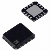
ADA4856-3YCPZ-R7 Analog Devices Inc, ADA4856-3YCPZ-R7 Datasheet - Page 14

ADA4856-3YCPZ-R7
Manufacturer Part Number
ADA4856-3YCPZ-R7
Description
Triple High Speed Extend Input Range RR
Manufacturer
Analog Devices Inc
Datasheet
1.ADA4856-3YCPZ-R7.pdf
(20 pages)
Specifications of ADA4856-3YCPZ-R7
Applications
Voltage Feedback
Output Type
Rail-to-Rail
Number Of Circuits
3
-3db Bandwidth
370MHz
Slew Rate
800 V/µs
Current - Supply
7.8mA
Current - Output / Channel
52mA
Voltage - Supply, Single/dual (±)
3 V ~ 5.5 V, ±1.5 V ~ 2.75 V
Mounting Type
Surface Mount
Package / Case
16-VQFN, CSP Exposed Pad
Lead Free Status / RoHS Status
Lead free / RoHS Compliant
Other names
ADA4856-3YCPZ-R7TR
ADA4856-3
USING THE ADA4856-3 IN GAINS EQUAL TO +3,
+4, AND +5
Depending on certain applications, it might be useful to have a
fixed gain amplifier that can provide various gains. The advantage
of having a fixed gain amplifier is the ease of layout, the reduced
number of components needed, and the matching of the gain
and feedback resistors.
Gain of +3 Configuration
Figure 38 shows the ADA4856-3 used as an amplifier with a
fixed gain of +3. No external resistors are required, just a simple
trace connecting certain inputs and outputs. Connect V
which is set to a gain of +2, and U2, which is set to unity. U3 then
takes the output of U1 and gains it up by +2 and subtracts the
output of U2 to produce V
signal frequency response for G = +3 is flat out to 65 MHz, with a
bandwidth of 165 MHz, a 2 V p-p output voltage, and a 100 Ω load.
Gain of +4 Configuration
To get a gain of +4, set one amplifier to a gain of +1 and set the
other two amplifiers to a gain of +2. Figure 39 shows V
U2 at unity, then U1 takes the output of U2 and gains it by +2, and
then feeds it to U3, which also gains it by +2 to produce V
V
V
IN
IN
PD
PD
1
2
3
4
1
2
3
4
ADA4856-3
ADA4856-3
16
Figure 38. Gain of +3
16
Figure 39. Gain of +4
5
5
OUT
15
15
6
6
. As shown in Figure 41, the large
14
14
7
7
–V
–V
–V
–V
13
13
8
8
S
S
S
S
12
11
10
12
11
10
0.1µF
0.1µF
9
9
0.1µF
0.1µF
0.1µF
0.1µF
+V
+V
+V
+V
0.1µF
+
0.1µF
+
10µF
10µF
S
V
S
V
S
S
+
+
OUT
OUT
IN
10µF
10µF
going in
OUT
IN
to U1,
.
Rev. A | Page 14 of 20
As shown in Figure 41, the large signal frequency response
for G = +4 is also flat out to 65 MHz, and it has a bandwidth
of 180 MHz.
Gain of +5 Configuration
The gain of +5 is very similar to the G = +3 configuration but with
U2 set to a gain of −1, which ends up being added to twice the
output of U1 to generate V
Figure 41 shows the large signal frequency response of the three
closed-loop gain sets (+3, +4, and +5) with flatness that extends
to 65 MHz and a −3 dB bandwidth of 190 MHz.
Figure 41. Large Signal Frequency Response for All Three Gains
–12
–15
–18
15
12
–3
–6
–9
V
9
6
3
0
IN
1
PD
R
V
V
L
S
OUT
1
2
3
4
= 100Ω
= 5V
= 2V p-p
ADA4856-3
Figure 40. Gain of +5
16
5
10
OUT
FREQUENCY (MHz)
15
6
G = +3
with G = +5.
14
7
–V
–V
13
8
S
S
G = +4
100
12
11
10
0.1µF
9
0.1µF
0.1µF
G = +5
+V
+V
0.1µF
+
10µF
S
V
S
+
OUT
10µF
1000


