ADAU1445YSVZ-3A-RL Analog Devices Inc, ADAU1445YSVZ-3A-RL Datasheet - Page 24
ADAU1445YSVZ-3A-RL
Manufacturer Part Number
ADAU1445YSVZ-3A-RL
Description
175MHZ SigmaDSP,2x8 SRCs
Manufacturer
Analog Devices Inc
Series
SigmaDSP®r
Type
Audio Processorr
Specifications of ADAU1445YSVZ-3A-RL
Applications
Automotive Audio
Mounting Type
Surface Mount
Package / Case
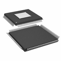
100-TQFP Exposed Pad, 100-eTQFP, 100-HTQFP, 100-VQFP
Format
Fixed Point
Program Memory Size
Not RequiredKB
Operating Supply Voltage (typ)
1.8/3.3V
Operating Temp Range
-40C to 105C
Operating Temperature Classification
Industrial
Mounting
Surface Mount
Pin Count
100
Lead Free Status / RoHS Status
Lead free / RoHS Compliant
Lead Free Status / RoHS Status
Lead free / RoHS Compliant
Available stocks
Company
Part Number
Manufacturer
Quantity
Price
Company:

Part Number:
ADAU1445YSVZ-3A-RL
Manufacturer:
Analog Devices Inc
Quantity:
10 000


ADAU1445/ADAU1446
CONTROL PORT
Overview
The ADAU1445/ADAU1446 can operate in one of three control
modes: I
(no external controller).
The ADAU1445/ADAU1446 have both a 4-wire SPI control port
and a 2-wire I
RAMs and registers. When the SELFBOOT pin is low at power-up,
the chip defaults to I
by pulling Pin CLATCH low three times. When the SELFBOOT
pin is set high at power-up, the ADAU1445/ADAU1446 load
the program, parameters, and register settings from an external
EEPROM at startup.
The control port is capable of full read and write operations for
all memories and registers, except for those that are read only.
Most signal processing parameters are controlled by writing
new values to the parameter RAM using the control port. Other
functions, such as mute and input/output mode control, are
programmed by writing to the registers.
All addresses can be accessed in either a single-word mode or a
burst mode. A control word consists of the chip address, the
register/RAM subaddress, and the data to be written. The
number of bytes per word depends on the type of data that is
being written.
The first byte (Byte 0) of a control word contains the 7-bit chip
address plus the R/ W bit. The next two bytes (Byte 1 and Byte 2)
together form the subaddress of the memory or register location
within the ADAU1445/ADAU1446. This subaddress must be
two bytes because the memory locations within the ADAU1445/
ADAU1446 are directly addressable, and their sizes exceed the
range of single-byte addressing. All subsequent bytes (starting
with Byte 3) contain the data, such as control port data, program
data, or parameter data. The exact formats for specific types of
writes are shown in
The ADAU1445/ADAU1446 have several mechanisms for
updating signal processing parameters in real time without causing
pops or clicks on the output. In cases where large blocks of data
must be downloaded, the output of the DSP core can be halted,
new data can be loaded, and then the output of the DSP core can be
restarted. This is typically done during the booting sequence at
startup or when loading a new program into RAM. In cases
where only a few parameters must be changed, they can be
loaded without halting the program. A software-based safeload
mechanism is included for this purpose, and it can be used to
buffer a full set of parameters (for example, the five coefficients
of a biquad) and then transfer these parameters into the active
program within one audio frame.
The control port pins are multifunctional according to the
mode in which the part is operating. Table 14 details these
functions.
2
C control mode, SPI control mode, or self-boot mode
2
C bus control port. Each can be used to set the
2
C mode but can be put into SPI control mode
Figure 13
and
Figure 19
.
Rev. A | Page 24 of 92
I
The ADAU1445/ADAU1446 support a 2-wire serial (I
compatible) microprocessor bus driving multiple peripherals.
Two pins, serial data (SDA) and serial clock (SCL), carry infor-
mation between the ADAU1445/ADAU1446 and the system I
master controller. In I
always slaves on the bus, which means that the parts cannot initiate
a data transfer.
Each slave device is recognized by a unique address. The address
bit sequence is shown in Table 11. The ADAU1445/ADAU1446
have eight possible slave addresses: four for writing operations
and four for reading. These are unique addresses for the device
and are illustrated in Table 12.
Users can communicate with these addresses by using the USBi
communication channel list in the hardware configuration tab
of SigmaStudio. The LSB of the byte sets either a read or write
operation; Logic Level 1 corresponds to a read operation, and
Logic Level 0 corresponds to a write operation. Address Bit 5 and
Address Bit 6 are set by tying the ADDRx pins of the ADAU1445/
ADAU1446 to Logic Level 0 or Logic Level 1. Both SDA and
SCL should have pull-up resistors on the lines connected to them
(a standard value is 2.0 kΩ, but this can be changed depending
on the capacitive load on the line). The voltage on these signal
lines should not be greater than the voltage of IOVDD (3.3 V).
Table 11. ADAU1445/ADAU1446 Address Bit Sequence
Bit 0
0
Table 12. ADAU1445/ADAU1446 I
ADDR1
0
0
0
0
1
1
1
1
1
Addressing
Initially, all devices on the I
the devices monitor the SDA and SCL lines for a start condition
and the proper address. The I
establishing a start condition, defined by a high-to-low transition
on SDA while SCL remains high. This indicates that an address or
an address and data stream follow. All devices on the bus respond
to the start condition and shift the next eight bits (7-bit address
+ R/ W bit) MSB first. The device that recognizes the transmitted
address responds by pulling the data line low during the ninth
clock pulse. This ninth bit is known as an acknowledge bit. All
other devices withdraw from the bus at this point and return to
2
0 = write, 1 = read.
C Port
Bit 1
1
ADDR0
0
0
1
1
0
0
1
1
Bit 2
1
Read/Write
0
1
0
1
0
1
0
1
2
C mode, the ADAU1445/ADAU1446 are
Bit 3
1
2
2
C bus are in an idle state, in which
C master initiates a data transfer by
Bit 4
0
1
Slave Address
0x70
0x71
0x72
0x73
0x74
0x75
0x76
0x77
2
C Slave Addresses
Bit 5
ADDR1
Bit 6
ADDR0
2
C
Bit 7
R/W
2
C
Related parts for ADAU1445YSVZ-3A-RL
Image
Part Number
Description
Manufacturer
Datasheet
Request
R

Part Number:
Description:
SigmaDSP� Digital Audio Processor with Flexible Audio Routing Matrix
Manufacturer:
Analog Devices
Datasheet:

Part Number:
Description:
±1.7g Dual-Axis IMEMS Accelerometer Evaluation Board
Manufacturer:
Analog Devices Inc
Datasheet:

Part Number:
Description:
Inertial Sensor Evaluation System
Manufacturer:
Analog Devices Inc
Datasheet:
Part Number:
Description:
Manufacturer:
Analog Devices Inc
Datasheet:
Part Number:
Description:
Manufacturer:
Analog Devices Inc
Datasheet:
Part Number:
Description:
Manufacturer:
Analog Devices Inc
Datasheet:
Part Number:
Description:
Manufacturer:
Analog Devices Inc
Datasheet:
Part Number:
Description:
Manufacturer:
Analog Devices Inc
Datasheet:
Part Number:
Description:
Manufacturer:
Analog Devices Inc
Datasheet:
Part Number:
Description:
Manufacturer:
Analog Devices Inc
Datasheet:
Part Number:
Description:
Manufacturer:
Analog Devices Inc
Datasheet:
Part Number:
Description:
Manufacturer:
Analog Devices Inc
Datasheet:
Part Number:
Description:
Manufacturer:
Analog Devices Inc
Datasheet: