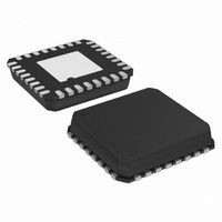
ADCMP566BCP Analog Devices Inc, ADCMP566BCP Datasheet - Page 10

ADCMP566BCP
Manufacturer Part Number
ADCMP566BCP
Description
HIGH SPEED COMPARATOR
Manufacturer
Analog Devices Inc
Type
with Latchr
Datasheet
1.ADCMP566BCPZ.pdf
(16 pages)
Specifications of ADCMP566BCP
Rohs Compliant
NO
Rohs Status
RoHS non-compliant
Number Of Elements
2
Output Type
Complementary, Differential, ECL, Open-Emitter
Voltage - Supply
±4.75 V ~ 5.25 V
Mounting Type
Surface Mount
Package / Case
32-LFCSP
For Use With
EVAL-ADCMP566BCPZ - BOARD EVALUATION ADCMP566BPZ
Lead Free Status / RoHS Status
ADCMP566
as the variation in propagation delay as the input overdrive
conditions are changed (Figure 4). For the ADCMP566,
overdrive dispersion is typically 35 ps as the overdrive is
changed from 100 mV to 1 V. This specification applies for
both positive and negative overdrive since the ADCMP566 has
equal delays for positive and negative going inputs.
The 35 ps propagation delay overdrive dispersion of the
ADCMP566 offers considerable improvement of the 100 ps
dispersion of other similar series comparators.
COMPARATOR HYSTERESIS
The addition of hysteresis to a comparator is often useful in a
noisy environment or where it is not desirable for the compara-
tor to toggle between states when the input signal is at the
switching threshold. The transfer function for a comparator
with hysteresis is shown in Figure 5. If the input voltage
approaches the threshold from the negative direction, the
comparator will switch from a 0 to a 1 when the input crosses
+V
comparator will remain in a 1 state until the threshold −V
crossed coming from the positive direction. In this manner,
noise centered on 0 V input will not cause the comparator to
switch states unless it exceeds the region bounded by ±V
Positive feedback from the output to the input is often used to
produce hysteresis in a comparator (Figure 9). The major
problem with this approach is that the amount of hysteresis
varies with the output logic levels, resulting in a hysteresis that
is not symmetrical around zero.
Another method to implement hysteresis is generated by
introducing a differential voltage between LATCH ENABLE
and LATCH ENABLE . inputs (Figure 10). Hysteresis generated
in this manner is independent of output swing and is symmetri-
cal around zero. The variation of hysteresis with input voltage is
shown in Figure 6.
H
/2. The new switching threshold becomes −V
INPUT VOLTAGE
Q OUTPUT
Figure 4. Propagation Delay Dispersion
1.5V OVERDRIVE
20mV OVERDRIVE
V
REF
DISPERSION
± V
OS
03633-0-004
H
/2. The
H
H
/2.
/2 is
Rev. 0 | Page 10 of 16
MINIMUM INPUT SLEW RATE REQUIREMENT
As for all high speed comparators, a minimum slew rate must
be met to ensure that the device does not oscillate when the
input crosses the threshold. This oscillation is due in part to the
high input bandwidth of the comparator and the parasitics of
the package. Analog Devices recommends a slew rate of 5 V/µs
or faster to ensure a clean output transition. If slew rates less
than 5 V/µs are used, then hysteresis should be added to reduce
the oscillation.
60
50
40
30
20
10
0
0
–20
Figure 5. Comparator Hysteresis Transfer Function
Figure 6. Comparator Hysteresis Transfer Function
–15
–V
2
H
–10
Using Latch Enable Input
∆ LATCH = LE – LEB (mV)
–5
0V
OUTPUT
0
+V
2
H
5
10
INPUT
03633-0-005
1
15


