ADDAC80-CCD-V Analog Devices Inc, ADDAC80-CCD-V Datasheet - Page 10
ADDAC80-CCD-V
Manufacturer Part Number
ADDAC80-CCD-V
Description
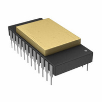
IC,D/A CONVERTER,SINGLE,12-BIT,BIPOLAR,DIP,24PIN
Manufacturer
Analog Devices Inc
Datasheet
1.ADDAC80NZ-CBI-V.pdf
(16 pages)
Specifications of ADDAC80-CCD-V
Rohs Status
RoHS non-compliant
Settling Time
2µs
Number Of Bits
12
Data Interface
Parallel
Number Of Converters
1
Voltage Supply Source
Dual ±
Power Dissipation (max)
300mW
Operating Temperature
0°C ~ 70°C
Mounting Type
Through Hole
Package / Case
24-CDIP (0.600", 15.24mm)
Lead Free Status / RoHS Status
Available stocks
Company
Part Number
Manufacturer
Quantity
Price


ADDAC80/ADDAC85/ADDAC87
Offset Adjustment
For unipolar (CSB) configurations, apply the digital input code
that should produce zero potential output and adjust the
OFFSET potentiometer for zero output. For bipolar (COB, CTC)
configurations, apply the digital input code that should produce
the maximum negative output voltage. Example: If the FULL
SCALE RANGE is connected for 20 V, the maximum negative
output voltage is –10 V. See Table II for corresponding codes.
Gain Adjustment
For either unipolar or bipolar configurations, apply the digital
input that should give the maximum positive voltage output.
Adjust the GAIN potentiometer for this positive full-scale voltage.
See Table II for positive full-scale voltages.
10
11
12
1
2
3
4
5
6
7
8
9
NETWORK
SWITCHES
RESISTOR
CURRENT
LADDER
12-BIT
AND
Digital Input
12-Bit Resolution
MSB
0 0 0 0 0 0 0 0 0 0 0 0
0 1 1 1 1 1 1 1 1 1 1 1
1 0 0 0 0 0 0 0 0 0 0 0
1 1 1 1 1 1 1 1 1 1 1 1
l LSB
To obtain values for other binary ranges 0 to 5 V range: divide 0 to 10 values by 2; ± 5 V range: divide
CONTROL
5k
± 10 V range values by 2; ± 2.5 V range: divide ± 10 V range values by 4.
CIRCUIT
REF
3k
6.3k
2k
24
23
22
21
20
19
18
17
16
15
14
13
10M
3.9M
LSB 0 to +10 V
0.01 F
1 F
1 F
Table II. Digital Input Analog Output
+9.9976 V
+5.0000 V
+4.9976 V
0.0000 V
2.44 mV
100k
100k
10k
10k
TO
TO
Voltage
+V
–V
+V
–V
S
S
S
S
Analog Output
+9.9951 V
0.0000 V
4.88 mV
–10.0000 V
–0.0049 V
10 V
10
11
12
1
2
3
4
5
6
7
8
9
0 to –2 mA
–1.9995 mA
–1.0000 mA
–0.9995 mA
0.0000 mA
0.488 µA
SWITCHES
RESISTOR
NETWORK
CURRENT
LADDER
12-BIT
AND
Current
3.9M
10M
5k
–
+
CONTROL
CIRCUIT
–0.9995 mA
0.0000 mA
+0.0005 mA
–1.00 mA
0.488 µA
REF
1 mA
6.3k
5k
270k
180k
24
23
22
21
20
19
18
17
16
15
14
13
270k
7.8k
180k
10k
10M
0.01 F
3.9M
1 F
1 F
100k
100k
10k
10k
TO
TO
–V
–V
+V
+V
S
S
S
S
Related parts for ADDAC80-CCD-V
Image
Part Number
Description
Manufacturer
Datasheet
Request
R

Part Number:
Description:
IC,D/A CONVERTER,SINGLE,12-BIT,BIPOLAR,DIP,24PIN
Manufacturer:
Analog Devices Inc
Datasheet:

Part Number:
Description:
Data Acquisition Products Catalog Supplement 1979
Manufacturer:
Analog Devices

Part Number:
Description:
±1.7g Dual-Axis IMEMS Accelerometer Evaluation Board
Manufacturer:
Analog Devices Inc
Datasheet:

Part Number:
Description:
Inertial Sensor Evaluation System
Manufacturer:
Analog Devices Inc
Datasheet:
Part Number:
Description:
Manufacturer:
Analog Devices Inc
Datasheet:
Part Number:
Description:
Manufacturer:
Analog Devices Inc
Datasheet:
Part Number:
Description:
Manufacturer:
Analog Devices Inc
Datasheet:
Part Number:
Description:
Manufacturer:
Analog Devices Inc
Datasheet:
Part Number:
Description:
Manufacturer:
Analog Devices Inc
Datasheet:
Part Number:
Description:
Manufacturer:
Analog Devices Inc
Datasheet:
Part Number:
Description:
Manufacturer:
Analog Devices Inc
Datasheet:
Part Number:
Description:
Manufacturer:
Analog Devices Inc
Datasheet: