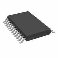
ADF7011BRU-REEL7 Analog Devices Inc, ADF7011BRU-REEL7 Datasheet

ADF7011BRU-REEL7
Specifications of ADF7011BRU-REEL7
Related parts for ADF7011BRU-REEL7
ADF7011BRU-REEL7 Summary of contents
Page 1
FEATURES Single Chip Low Power UHF Transmitter Frequency Band 433 MHz to 435 MHz 868 MHz to 870 MHz On-Chip VCO and Fractional-N PLL 2 3.6 V Supply Voltage Programmable Output Power –16 dBm to +12 dBm, 0.3 ...
Page 2
ADF7011–SPECIFICATIONS Parameter RF CHARACTERISTICS Output Frequency Ranges Lower SRD Band Upper SRD Band Phase Frequency Detector Frequency TRANSMISSION PARAMETERS 2 Transmit Rate FSK ASK GFSK Frequency Shift Keying 3 FSK Separation Gaussian Filter t Amplitude Shift Keying Depth On/Off Keying ...
Page 3
Parameter PHASE-LOCKED LOOP VCO Gain 433 MHz/868 MHz 5 Phase Noise (In-Band) 433 MHz 6 Phase Noise (Out-of-Band) 7 Phase Noise (In-Band) 868 MHz 8 Phase Noise (Out-of-Band Spurious 47–74, 87.5–118, 174–230, 470–862 MHz 9 kHz – 1 ...
Page 4
... This device is a high performance RF integrated circuit with an ESD rating of <1 kV and is ESD sensitive. Proper precautions should be taken for handling and assembly. 3 GND = VCOGND = CPGND = RFGND = DGND = AGND = 0 V. Model ADF7011BRU ADF7011BRU-REEL ADF7011BRU-REEL7 –4– DB0 (LSB) DB1 (CONTROL BIT C1 ORDERING GUIDE ...
Page 5
Pin No. Mnemonic Function 1 R External Resistor to Set Change Pump Current and Some Internal Bias Currents. Use 4.7 kΩ as default: SET = I CP MAX So, with R SET 2 CPV Charge Pump Supply. This should be ...
Page 6
ADF7011 Pin No. Mnemonic Function 15 OSC1 Oscillator Pin. For use with crystal reference only. This is three-stated when an external reference oscilla- tor is used. 16 VCO Voltage Controlled Oscillator Ground. GND 17 TEST Input to the RF Fractional-N ...
Page 7
RL = 10.0dBm PFD FREQUENCY = 19.2MHz LOOP BW = 100kHz RBW = 1kHz 868.3MHz TPC 1. FSK Modulated Signal, F Data Rate = 19.2 kbps, 10 dBm RL = 10.0dBm –2dBm ...
Page 8
ADF7011 C1 RISE 144.8ns C1 FALL 145.6ns C1 +DUTY 49.385% Ch1 500mV M 200ns TPC 7. 1.6 MHz CLOCK OUT +10dBm PFD FREQUENCY = 19.2MHz LOOP BW = 100kHz RBW = 10Hz +1.6MHz –53dBc 868.3MHz TPC ...
Page 9
REGISTER MAPS CLK RESERVED OUT DB23 DB22 DB21 DB20 DB19 DB18 DB17 DB16 DB15 DB14 DB13 DB12 DB11 DB10 DB9 R2 R1 CL4 CL3 CL2 CL1 X1 8-BIT INTEGER-N DB23 DB22 DB21 DB19 DB18 DB17 DB16 DB15 DB14 DB13 DB12 ...
Page 10
ADF7011 RF R Register CLK RESERVED OUT DB23 DB22 DB21 DB20 DB19 DB18 DB17 DB16 DB15 DB14 DB13 DB12 DB11 DB10 DB9 R2 R1 CL4 CL3 CL2 CL1 X1 XOE X1 0 XTAL OSCILLATOR ON 1 XTAL OSCILLATOR OFF CL3 ...
Page 11
RF N Register 8-BIT INTEGER-N DB19 DB18 DB17 DB16 DB15 DB14 DB13 DB12 DB11 DB10 DB23 DB22 DB21 DB20 LDP M12 ...
Page 12
ADF7011 Modulation Register INDEX GFSK MOD COUNTER CONTROL DB23 DB22 DB21 DB20 DB19 DB18 P1 IC2 IC1 MC3 MC2 MC1 IF AMPLITUDE SHIFT KEYING SELECTED, TxDATA = ...
Page 13
Function Register TEST MODES DB23 DB22 DB21 DB20 DB19 DB18 DB17 DB16 ...
Page 14
ADF7011 Default Values for Registers RESERVED CLK OUT DB21 DB20 DB19 DB18 DB17 DB16 DB15 DB14 DB13 DB12 DB11 DB10 DB9 DB23 DB22 8-BIT INTEGER-N DB23 DB22 DB19 DB18 DB17 DB16 DB15 DB14 ...
Page 15
CIRCUIT DESCRIPTION Reference Input Section The on-board crystal oscillator circuitry (Figure 2), allows the use of an inexpensive quartz crystal as the PLL reference. The oscillator circuit is enabled by setting XOE low enabled by default on power-up ...
Page 16
ADF7011 REGULATOR READY DIGITAL LOCK DETECT ANALOG LOCK DETECT R COUNTER/2 OUTPUT N COUNTER/2 OUTPUT R COUNTER OUTPUT N COUNTER OUTPUT Digital Lock Detect Digital lock detect is active high. The lock detect circuit is con- tained at the PFD. ...
Page 17
Voltage Controlled Oscillator (VCO) An on-chip VCO is included on the transmitter. The VCO con- verts the control voltage generated by the loop filter into an output frequency that is sent to the antenna via the power amplifier (PA). The ...
Page 18
ADF7011 0.00 0.20 0.50 1.00 0.0 25 – j2.6 433MHz 0.20 150 16 – j33 140 868MHz 0.50 130 120 1.00 110 100 80 90 Figure 10. Output Impedance on Smith Chart Fractional-N N Counter and Error Correction The ADF7011 ...
Page 19
MODULATION SCHEMES Frequency Shift Keying (FSK) Frequency shift keying is implemented by setting the N value for the center frequency and then toggling this with the TxDATA line. The deviation from the center frequency is set using Bits D1–D7 in ...
Page 20
ADF7011 APPLICATION EXAMPLES Application Example 1 Operating Frequency 433.92 MHz Output Power +10 dBm Current Consumption <30 mA Modulation ASK/FSK This system should be set up as shown Figure 15. The spurious levels using a crystal frequency of 4 MHz ...
Page 21
VCO IN LOCK DETECT 2MH CLOCK Z Figure 15. Application Diagram—433 MHz Operation with +10 dBm Output Power 4.7k VCO IN LOCK DETECT 4.84MH CLOCK Z Figure 16. Application Diagram—868 MHz Operation with +3 dBm Output Power REV. 0 ...
Page 22
ADF7011 4.7k VCO IN LOCK DETECT 4.84MH CLOCK Z Figure 17. Application Diagram—868 MHz Operation with +10 dBm Output Power 2.2 F 220nF CPV VCO REG R SET 12nH RF OUT CP VCO OUT IN ...
Page 23
Thin Shrink Small Outline Package [TSSOP] PIN 1 0.15 0.05 REV. 0 OUTLINE DIMENSIONS (RU-24) Dimensions shown in millimeters 7.90 7.80 7. 4.50 4.40 4.30 6.40 BSC 1 12 0.65 1.20 BSC MAX 8 0.30 0 0.20 ...
Page 24
–24– ...


