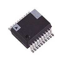
ADG467BRSZ-REEL Analog Devices Inc, ADG467BRSZ-REEL Datasheet - Page 8

ADG467BRSZ-REEL
Manufacturer Part Number
ADG467BRSZ-REEL
Description
Octal Channel Protector I.C.
Manufacturer
Analog Devices Inc
Series
ADG467r
Specifications of ADG467BRSZ-REEL
Voltage - Clamping
±40V
Technology
Mixed Technology
Number Of Circuits
8
Applications
General Purpose
Package / Case
20-SSOP
Operating Temperature (min)
-40C
Operating Temperature (max)
85C
Operating Temperature Classification
Industrial
Mounting
Surface Mount
Pin Count
20
Lead Free Status / RoHS Status
Lead free / RoHS Compliant
Power (watts)
-
Voltage - Working
-
Lead Free Status / Rohs Status
Compliant
Available stocks
Company
Part Number
Manufacturer
Quantity
Price
Part Number:
ADG467BRSZ-REEL
Manufacturer:
ADI/亚德诺
Quantity:
20 000
ADG466/ADG467
When a negative overvoltage is applied to the channel protector
circuit, the PMOS transistor enters a saturated mode of opera-
tion as the drain voltage exceeds V
low. As in the case of the positive overvoltage, the other MOS
devices are nonsaturated.
The channel protector is also functional when the supply rails
are down (e.g., power failure) or momentarily unconnected
(e.g., rack system). This is where the channel protector has an
advantage over more conventional protection methods such as
diode clamping (see Applications Information). When V
V
subnano-ampere levels (see Figure 21).
Figure 20. Negative Overvoltage on the Channel Protector
Figure 21. Channel Protector Supplies Equal to Zero Volts
SS
OVERVOLTAGE
equal 0 V, all transistors are off and the current is limited to
*V
OVERVOLTAGE
TP
NEGATIVE
POSITIVE OR
= PMOS THRESHOLD VOLTAGE (–2V)
NEGATIVE
(–20V)
SATURATED
NON-
V
DD
NMOS
OFF
(+15V)
V
NMOS
DD
OVERVOLTAGE
(0V)
NEGATIVE
SATURATED
(–20V)
V
SS
SS
PMOS
OFF
(–15V)
V
– V
PMOS
SS
(0V)
TP
. See Figure 20 be-
(0V)
V
SS
(–13V)
V
– V
DD
NMOS
OFF
TP
V
(+15V)
NMOS
DD
*
NON-
SATURATED
(0V)
DD
and
–8–
TRENCH ISOLATION
The MOS devices that make up the channel protector are iso-
lated from each other by an oxide layer (trench) (see Figure 22).
When the NMOS and PMOS devices are not electrically iso-
lated from each other, there exists the possibility of “latch-up”
caused by parasitic junctions between CMOS transistors. Latch-
up is caused when P-N junctions that are normally reverse bi-
ased become forward biased, causing large currents to flow,
which can be destructive.
CMOS devices are normally isolated from each other by Junc-
tion Isolation. In Junction Isolation, the N and P wells of the
CMOS transistors form a diode that is reverse-biased under
normal operation. However, during overvoltage conditions, this
diode becomes forward biased. A Silicon-Controlled Rectifier
(SCR) type circuit is formed by the two transistors causing a
significant amplification of the current that, in turn, leads to
latch-up. With Trench Isolation, this diode is removed; the
result is a latch-up proof circuit.
R
N
C
H
T
E
P +
N –
V
S
P-CHANNEL
Figure 22. Trench Isolation
V
G
SUBSTRATE (BACKGATE)
BURIED OXIDE LAYER
V
P +
D
R
N
C
H
T
E
N +
V
P –
S
N-CHANNEL
V
G
REV. A
N +
V
D
R
N
C
H
T
E


