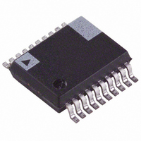
ADM1385ARS Analog Devices Inc, ADM1385ARS Datasheet - Page 3

ADM1385ARS
Manufacturer Part Number
ADM1385ARS
Description
LOW POWER, 3V, RS-232 I.C.
Manufacturer
Analog Devices Inc
Type
Transceiverr
Datasheet
1.ADM3202ARUZ.pdf
(12 pages)
Specifications of ADM1385ARS
Rohs Compliant
NO
Rohs Status
RoHS non-compliant
Number Of Drivers/receivers
2/2
Protocol
RS232
Voltage - Supply
3 V ~ 3.6 V
Mounting Type
Surface Mount
Package / Case
20-SSOP
Lead Free Status / RoHS Status
Available stocks
Company
Part Number
Manufacturer
Quantity
Price
Company:
Part Number:
ADM1385ARS
Manufacturer:
AD
Quantity:
303
Part Number:
ADM1385ARS
Manufacturer:
ADI/亚德诺
Quantity:
20 000
Company:
Part Number:
ADM1385ARSZ
Manufacturer:
ADI
Quantity:
10
Part Number:
ADM1385ARSZ
Manufacturer:
ADI/亚德诺
Quantity:
20 000
SPECIFICATIONS
V
Table 1.
Parameter
DC CHARACTERISTICS
LOGIC
RS-232 RECEIVER
RS-232 TRANSMITTER
TIMING CHARACTERISTICS
1
ADM1385: Input leakage current typically −10 μA when T
CC
Operating Voltage Range
V
Shutdown Supply Current
Input Logic Threshold Low, V
Input Logic Threshold High, V
CMOS Output Voltage Low, V
CMOS Output Voltage High, V
Logic Pull-Up Current
Output Leakage Current
EIA-232 Input Voltage Range
EIA-232 Input Threshold Low
EIA-232 Input Threshold High
EIA-232 Input Hysteresis
EIA-232 Input Resistance
Output Voltage Swing (RS-232)
Output Voltage Swing (RS-562)
Transmitter Output Resistance
RS-232 Output Short-Circuit Current
Output Leakage Current
Maximum Data Rate
Receiver Propagation Delay
Transmitter Propagation Delay
Receiver Output Enable Time
Receiver Output Disable Time
Transmitter Skew
Receiver Skew
Transition Region Slew Rate
CC
= 3.3 V ± 0.3 V, C1 to C4 = 0.1 μF. All specifications T
TPHL
TPLH
Power Supply Current
INL
OL
INH
OH
Min
3.0
2.0
V
−30
0.6
3
±5.0
±3.7
300
460
5.5
CC
− 0.6
IN
= GND.
Typ
3.3
1.3
8
0.01
5
1.2
1.6
0.4
5
±5.2
±15
0.4
0.4
0.3
200
200
30
300
10
MIN
Max
5.5
3
12
0.5
0.8
0.4
10
±10
+30
2.4
7
±25
1
1
1.2
30
Rev. D | Page 3 of 12
to T
MAX
Unit
V
mA
mA
μA
V
V
V
V
μA
μA
V
V
V
V
kΩ
V
V
Ω
mA
μA
kbps
μs
μs
μs
ns
ns
ns
ns
V/μs
, unless otherwise noted.
No load
Test Conditions/Comments
R
T
T
I
I
T
Receivers disabled
V
V
V
SD = low, V
V
Tx switching
R
Measured from +3 V to −3 V or −3 V to +3 V, V
R
OUT
OUT
IN
IN
IN
L
CC
CC
CC
CC
L
L
= 3 kΩ to GND
= 3 kΩ, C
= 3 kΩ, C
= GND to V
= 3.3 V, all transmitter outputs loaded with 3 kΩ to ground
= 3.0 V
= 0 V, V
= 3.3 V, R
= 1.6 mA
= −1 mA
OUT
OUT
L
L
L
= 1000 pF
= 1000 pF, T
= 3 kΩ to 7 kΩ, C
= ±2 V
CC
= 12 V
ADM3202/ADM3222/ADM1385
1
A
= 25°C
L
= 50 pF to 1000 pF, one
CC
= +3.3 V;


