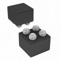
ADP120-ACBZ18R7 Analog Devices Inc, ADP120-ACBZ18R7 Datasheet - Page 17

ADP120-ACBZ18R7
Manufacturer Part Number
ADP120-ACBZ18R7
Description
100mA Low Current Low Iq LDO Vout=1.8v
Manufacturer
Analog Devices Inc
Datasheet
1.ADP120-12-EVALZ.pdf
(20 pages)
Specifications of ADP120-ACBZ18R7
Regulator Topology
Positive Fixed
Voltage - Output
1.8V
Voltage - Input
2.3 ~ 5.5 V
Number Of Regulators
1
Current - Output
100mA
Current - Limit (min)
110mA
Operating Temperature
-40°C ~ 125°C
Mounting Type
Surface Mount
Package / Case
4-WLCSP
Lead Free Status / RoHS Status
Lead free / RoHS Compliant
Voltage - Dropout (typical)
-
Lead Free Status / RoHS Status
Lead free / RoHS Compliant
In cases where the board temperature is known, use the thermal
characterization parameter, Ψ
perature rise. Maximum junction temperature (T
from the board temperature (T
using the formula
PCB LAYOUT CONSIDERATIONS
Improve heat dissipation from the package by increasing the
amount of copper attached to the pins of the ADP120. However,
as listed in Table 6, a point of diminishing return is eventually
reached, beyond which an increase in the copper size does
not yield significant heat dissipation benefits.
Place the input capacitor as close as possible to the VIN and
GND pins. Place the output capacitor as close as possible to the
VOUT and GND pins. Use of 0402- or 0603-size capacitors and
resistors achieves the smallest possible footprint solution on
boards where area is limited.
T
J
140
120
100
140
120
100
= T
80
60
40
20
80
60
40
20
0
0
0.5
0.5
B
MAX JUNCTION TEMPERATURE
MAX JUNCTION TEMPERATURE
+ (P
I
1.0
LOAD
1.0
D
× Ψ
I
= 100mA
LOAD
Figure 47. WLCSP, T
1.5
1.5
Figure 46. TSOT, T
JB
)
= 100mA
I
LOAD
2.0
2.0
I
LOAD
= 1mA
V
V
IN
IN
JB
I
LOAD
B
, to estimate the junction tem-
I
– V
= 75mA
– V
) and power dissipation (P
LOAD
2.5
2.5
OUT
OUT
I
= 25mA
LOAD
= 75mA
B
I
(V)
(V)
B
LOAD
= 85°C
= 85°C
3.0
3.0
= 10mA
I
LOAD
= 10mA
I
LOAD
3.5
3.5
= 50mA
I
LOAD
I
LOAD
= 50mA
J
) is calculated
4.0
4.0
= 25mA
= 1mA
4.5
4.5
D
)
Rev. B | Page 17 of 20
(5)
GND
GND
VIN
Figure 50. WLCSP PCB Layout—Bottom Side
Figure 49. WLCSP PCB Layout—Top Side
J1
Figure 48. TSOT PCB Layout
EN
ANALOG DEVICES
ADP120-xx-EVALZ
C1
U1
C2
VOUT
GND
GND
ADP120


