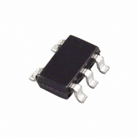
ADP150AUJZ-2.8-R7 Analog Devices Inc, ADP150AUJZ-2.8-R7 Datasheet - Page 14

ADP150AUJZ-2.8-R7
Manufacturer Part Number
ADP150AUJZ-2.8-R7
Description
150mA Ultra-Low Noise LDO 2.8 Vout
Manufacturer
Analog Devices Inc
Datasheet
1.ADP150-BL1-EVZ.pdf
(20 pages)
Specifications of ADP150AUJZ-2.8-R7
Design Resources
Broadband Low EVM Direct Conversion Transmitter (CN0134) Broadband Low EVM Direct Conversion Transmitter Using LO Divide-by-2 Modulator (CN0144) Using low noise linear drop-out regulators to power wideband PLL & VCO IC's (CN0147)
Regulator Topology
Positive Fixed
Voltage - Output
2.8V
Voltage - Input
Up to 5.5V
Voltage - Dropout (typical)
0.105V @ 150mA
Number Of Regulators
1
Current - Output
150mA (Max)
Current - Limit (min)
190mA
Operating Temperature
-40°C ~ 125°C
Mounting Type
Surface Mount
Package / Case
TSOT-23-5, TSOT-5, TSOP-5
Lead Free Status / RoHS Status
Lead free / RoHS Compliant
Other names
ADP150AUJZ-2.8-R7TR
Available stocks
Company
Part Number
Manufacturer
Quantity
Price
Part Number:
ADP150AUJZ-2.8-R72
Manufacturer:
ADI/亚德诺
Quantity:
20 000
ADP150
THERMAL CONSIDERATIONS
In most applications, the ADP150 does not dissipate much heat
due to its high efficiency. However, in applications with high
ambient temperature and high supply voltage to output voltage
differential, the heat dissipated in the package is large enough
that it can cause the junction temperature of the die to exceed
the maximum junction temperature of 125°C.
When the junction temperature exceeds 150°C, the converter
enters thermal shutdown. It recovers only after the junction
temperature decreases below 135°C to prevent any permanent
damage. Therefore, thermal analysis for the chosen application is
very important to guarantee reliable performance over all conditions.
The junction temperature of the die is the sum of the ambient
temperature of the environment and the temperature rise of the
package due to the power dissipation, as shown in Equation 2.
To guarantee reliable operation, the junction temperature of
the ADP150 must not exceed 125°C. To ensure that the junction
temperature stays below 125°C, be aware of the parameters that
contribute to the junction temperature changes. These parameters
include ambient temperature, power dissipation in the power
device, and thermal resistances between the junction and
ambient air (θ
assembly compounds that are used and the amount of copper
used to solder the package GND pins to the PCB. Table 7 shows
typical θ
for various PCB copper sizes. Table 8 shows the typical Ψ
value of the 5-lead TSOT and 4-ball WLCSP.
Table 7. Typical θJA Values
Copper Size (mm
0
50
100
300
500
1
Table 8. Typical Ψ
TSOT
42.8
Use Equation 2 to calculate the junction temperature.
where:
T
P
where:
I
I
V
LOAD
GND
Device soldered to minimum size pin traces.
1
D
A
IN
is the power dissipation in the die, given by
is the ambient temperature.
and V
is the ground current.
T
P
is the load current.
J
D
= T
= [(V
JA
values of the 5-lead TSOT and 4-ball WLCSP packages
OUT
A
+ (P
IN
are input and output voltages, respectively.
JA
− V
). The θ
D
2
× θ
)
OUT
JB
Values
JA
) × I
)
JA
number is dependent on the package
LOAD
Ψ
JB
] + (V
WLCSP
58.4
(°C/W)
TSOT
170
152
146
134
131
IN
× I
GND
θ
)
JA
(°C/W)
WLCSP
260
159
157
153
151
JB
Rev. A | Page 14 of 20
(2)
Power dissipation due to ground current is quite small and can be
ignored. Therefore, the junction temperature equation simplifies to
As shown in the previous equation, for a given ambient temperature,
input-to-output voltage differential, and continuous load current,
there exists a minimum copper size requirement for the PCB to
ensure that the junction temperature does not rise above 125°C.
Figure 33 to Figure 46 show the junction temperature calculations
for the different ambient temperatures, load currents, V
differentials, and areas of PCB copper.
T
140
120
100
140
120
100
J
80
60
40
20
80
60
40
20
= T
0
0
0.5
0.5
A
Figure 33. TSOT, 500 mm
Figure 34. TSOT, 100 mm
+ {[(V
MAX JUNCTION TEMPERATURE
I
I
I
I
I
I
I
MAX JUNCTION TEMPERATURE
I
I
I
I
I
I
I
LOAD
LOAD
LOAD
LOAD
LOAD
LOAD
LOAD
LOAD
LOAD
LOAD
LOAD
LOAD
LOAD
LOAD
1.0
1.0
= 1mA
= 10mA
= 25mA
= 50mA
= 75mA
= 100mA
= 150mA
= 1mA
= 10mA
= 25mA
= 50mA
= 75mA
= 100mA
= 150mA
IN
1.5
1.5
− V
OUT
2.0
2.0
) × I
V
V
IN
IN
– V
– V
2
2
LOAD
2.5
2.5
of PCB Copper, T
of PCB Copper, T
OUT
OUT
] × θ
(V)
(V)
3.0
3.0
JA
}
3.5
3.5
A
A
= 25°C
= 25°C
4.0
4.0
IN
-to-V
4.5
4.5
OUT
(3)


