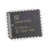
AM29F002BT-70JC Spansion Inc., AM29F002BT-70JC Datasheet - Page 24

AM29F002BT-70JC
Manufacturer Part Number
AM29F002BT-70JC
Description
Flash Memory IC
Manufacturer
Spansion Inc.
Datasheets
1.AM29F002BT-70JC.pdf
(42 pages)
2.AM29F002BT-70JC.pdf
(42 pages)
3.AM29F002BT-70JC.pdf
(40 pages)
Specifications of AM29F002BT-70JC
Memory Size
2Mbit
Memory Configuration
256K X 8
Ic Interface Type
Parallel
Access Time
70ns
Memory Case Style
PLCC
No. Of Pins
32
Operating Temperature Range
0°C To +70°C
Termination Type
SMD
Available stocks
Company
Part Number
Manufacturer
Quantity
Price
Company:
Part Number:
AM29F002BT-70JC
Manufacturer:
AMD
Quantity:
3 366
ABSOLUTE MAXIMUM RATINGS
S to rag e Te m pe ratur e
P las tic Pa ck a ge s . . . . . . . . . . . . . . . – 65
A m bie nt Te m per ature
w ith Pow e r App lied . . . . . . . . . . . . . . – 55
Voltag e w ith R es pe c t to Gr oun d
O utpu t Sh or t C ir cu it C u rre nt ( N ote 3) . . . . . . 20 0 m A
No tes:
1. Minimum DC voltage on input or I/O pins is –0.5 V. During
2. Minimum DC input voltage on pins A9, OE#, and RESET#
3. No more than one output can be shorted to ground at a
Stresses above those listed under “Absolute Maximum
Ratings” can cause permanent damage to the device. This is
a stress rating only; functional operation of the device at
these or any other conditions above those indicated in the
operational sections of this data sheet is not implied.
Exposure of the device to absolute maximum rating
conditions for extended periods can affect device reliability.
OPERAT ING RANGES
C o m m e rc ia l (C ) D e vices
A m bie nt Te m per ature ( T
In d u str ial ( I) D e vices
A m bie nt Te m per ature ( T
E xte n de d ( E) D ev ic es
A m bie nt Te m per ature ( T
V
V
V
Operating ranges define those limits between which the func-
tionality of the device is guaranteed.
2 2
CC
CC
CC
voltage transitions, input or I/O pins can overshoot V
–2.0 V for periods of up to 20 ns. See
DC voltage on input or I/O pins is
voltage transitions, input or I/O pins can overshoot to V
+2.0 V for periods up to 20 ns. See
is –0.5 V. During voltage transitions, A9, OE#, and
RESET# can overshoot V
20 ns. See
is +12.5 V which can overshoot to +13.5 V for periods up
to 20 ns. (RESET# is not available on Am29F002NB)
time. Duration of the short circuit should not be greater
than one second.
V
A9 , OE # , and
R ES ET # (N o te 2 ). . . . . . . . . . . .– 2.0 V to +1 2.5 V
All oth er pin s ( N ote 1) . . . . . . . . .–0.5 V to + 7.0 V
S u p p ly Vo ltag e s
for ± 5% d ev ic es . . . . . . . . . . .+4 .7 5 V to +5 .2 5 V
for ± 10% dev ic es . . . . . . . . . . . . + 4.5 V to + 5.5 V
C C
(N o te 1 ) . . . . . . . . . . . . . . . .–2.0 V to + 7.0 V
Figure
6. Maximum DC input voltage on pin A9
A
A
A
) . . . . . . . . . . . 0 ° C to + 70 °C
) . . . . . . . . . –40 °C to + 85 °C
) . . . . . . . . – 55° C to +1 25 °C
S S
to –2.0 V for periods of up to
V
C C
Figure
Figure
+0.5 V. During
°
°
C to +1 50
C to +1 25
7.
6. Maximum
A m 29 F 002 B /A m 29 F 00 2N B
S S
°
°
C C
to
C
C
+2.0 V
+0.5 V
+0.8 V
–0.5 V
–2.0 V
2.0 V
V
V
C C
C C
F ig u re 6 .
F ig ur e 7 .
O ve rs h o ot W av efo r m
Ove rs h o o t Wa vefo r m
20 ns
20 ns
M a xim u m N e g ative
M a xim u m Po s it iv e
20 ns
20 ns
20 ns
20 ns


