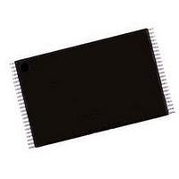
AM29F032B-90EC Spansion Inc., AM29F032B-90EC Datasheet - Page 10

AM29F032B-90EC
Manufacturer Part Number
AM29F032B-90EC
Description
Flash Memory IC
Manufacturer
Spansion Inc.
Datasheets
1.AM29F032B-90EI.pdf
(39 pages)
2.AM29F032B-90EC.pdf
(39 pages)
3.AM29F032B-90EI.pdf
(39 pages)
Specifications of AM29F032B-90EC
Memory Size
32Mbit
Memory Configuration
4M X 8
Ic Interface Type
Parallel
Access Time
90ns
Memory Case Style
TSOP
No. Of Pins
40
Operating Temperature Range
0°C To +70°C
Termination Type
SMD
Lead Free Status / RoHS Status
Contains lead / RoHS non-compliant
Available stocks
Company
Part Number
Manufacturer
Quantity
Price
Company:
Part Number:
AM29F032B-90EC
Manufacturer:
SPANSION
Quantity:
1 200
DEVICE BUS OPERATIONS
This section describes the requirements and use of the
device bus operations, which are initiated through the
internal command register. The command register it-
self does not occupy any addressable memory loca-
tion. The register is composed of latches that store the
commands, along with the address and data informa-
tion needed to execute the command. The contents of
Legend:
L = Logic Low = V
Note: See the sections Sector Group Protection and Temporary Sector Unprotect for more information.
Requirements for Reading Array Data
To read array data from the outputs, the system must
drive the CE# and OE# pins to V
control and selects the device. OE# is the output con-
trol and gates array data to the output pins. WE#
should remain at V
The internal state machine is set for reading array data
upon device power-up, or after a hardware reset. This
ensures that no spurious alteration of the memory
content occurs during the power transition. No com-
mand is necessary in this mode to obtain array data.
Standard microprocessor read cycles that assert valid
addresses on the device address inputs produce valid
data on the device data outputs. The device remains
enabled for read access until the command register
contents are altered.
See
mation. Refer to the AC Read Operations table for tim-
ing specifications and to
timing waveforms. I
represents the active current specification for reading
array data.
Writing Commands/Command Sequences
To write a command or command sequence (which in-
cludes programming data to the device and erasing
8
Read
Write
CMOS Standby
TTL Standby
Output Disable
Hardware Reset
Temporary Sector Unprotect
(See Note)
“Reading Array Data” on page 13
Operation
IL
, H = Logic High = V
IH
CC1
.
in the DC Characteristics table
Figure 9, on page 25
Table 1. Am29F032B Device Bus Operations
IL
. CE# is the power
IH
, V
V
CC
ID
for more infor-
CE#
= 12.0 ± 0.5 V, X = Don’t Care, D
± 0.5 V
H
X
X
L
L
L
D A T A
for the
Am29F032B
OE#
H
X
X
H
X
X
L
S H E E T
the register serve as inputs to the internal state ma-
chine. The state machine outputs dictate the function of
the device. The appropriate device bus operations
table lists the inputs and control levels required, and the
resulting output. The following subsections describe
each of these operations in further detail.
sectors of memory), the system must drive WE# and
CE# to V
An erase operation can erase one sector, multiple sec-
tors, or the entire device. The Sector Address Tables
indicate the address space that each sector occupies.
A “sector address” consists of the address bits re-
quired to uniquely select a sector. See the “Writing
specific address and data commands or sequences
into the command register initiates device operations.
The Command Definitions table defines the valid reg-
ister command sequences. Writing incorrect address
and data values or writing them in the improper se-
quence resets the device to reading array data.” sec-
tion for details on erasing a sector or the entire chip, or
suspending/resuming the erase operation.
After the system writes the autoselect command se-
quence, the device enters the autoselect mode. The
system can then read autoselect codes from the inter-
nal register (which is separate from the memory array)
on DQ7–DQ0. Standard read cycle timings apply in
this mode. Refer to the
and
sections for more information.
I
resents the active current specification for the write
mode. The
WE#
CC2
H
X
X
H
X
X
L
“Autoselect Command Sequence” on page 14
in the
IL
V
, and OE# to V
IN
“DC Characteristics” on page 23
RESET#
CC
““AC Characteristics” on page 25
= Data In, D
V
± 0.5 V
H
H
H
H
L
ID
“Autoselect Mode” on page 11
OUT
IH
.
= Data Out, A
A0–A21
21610D5 November 2, 2006
A
A
A
X
X
X
X
IN
IN
IN
IN
DQ0–DQ7
= Address In
High-Z
High-Z
High-Z
High-Z
D
table rep-
D
D
OUT
IN
IN
section


