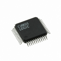
CS5366-DQZ Cirrus Logic Inc, CS5366-DQZ Datasheet - Page 31

CS5366-DQZ
Manufacturer Part Number
CS5366-DQZ
Description
IC,A/D CONVERTER,HEX,24-BIT,QFP,48PIN
Manufacturer
Cirrus Logic Inc
Datasheet
1.CS5366-CQZ.pdf
(42 pages)
Specifications of CS5366-DQZ
Number Of Bits
24
Sampling Rate (per Second)
216k
Data Interface
Serial
Number Of Converters
1
Power Dissipation (max)
830mW
Voltage Supply Source
Analog and Digital
Operating Temperature
-40°C ~ 105°C
Mounting Type
Surface Mount
Package / Case
48-LQFP
Lead Free Status / RoHS Status
Lead free / RoHS Compliant
For Use With
598-1549 - BOARD EVAL FOR CS5366 192KHZ ADC
Lead Free Status / RoHS Status
Lead free / RoHS Compliant
Other names
598-1698
Available stocks
Company
Part Number
Manufacturer
Quantity
Price
Company:
Part Number:
CS5366-DQZ
Manufacturer:
Cirrus Logic Inc
Quantity:
135
Company:
Part Number:
CS5366-DQZR
Manufacturer:
Cirrus Logic Inc
Quantity:
10 000
DS626F4
4.13.2 I²C Mode
In I²C Mode, SDA is a bidirectional data line. Data is clocked into and out of the part by the clock, SCL.
There is no CS pin. Pins AD0 and AD1 form the two least-significant bits of the chip address and should
be connected through a resistor to VLC or DGND, as desired. The state of the pins is latched when the
CS5366 is being released from RST.
A Start condition is defined as a falling transition of SDA while SCL is high. A Stop condition is a rising tran-
sition of SDA while SCL is high. All other transitions of SDA occur while SCL is low. The first byte sent to
the CS5366 after a Start condition consists of a 7-bit chip address field and a R/W bit (high for a read, low
for a write). The upper five bits of the 7-bit address field are fixed at 10011. To communicate with a CS5366,
the chip address field, which is the first byte sent to the CS5366, should match 10011 and be followed by
the settings of the AD1 and AD0. The eighth bit of the address is the R/W bit. If the operation is a write, the
next byte is the Memory Address Pointer (MAP), which selects the register to be read or written. If the op-
eration is a read, the contents of the register pointed to by the MAP will be output. Setting the auto-incre-
ment bit in MAP allows successive reads or writes of consecutive registers. Each byte is separated by an
acknowledge bit. The ACK bit is output from the CS5366 after each input byte is read and is input to the
CS5366 from the microcontroller after each transmitted byte.
Since the read operation cannot set the MAP, an aborted write operation is used as a preamble. The write
operation is aborted after the acknowledge for the MAP byte by sending a Stop condition. The following
pseudocode illustrates an aborted write operation followed by a read operation.
Send start condition.
Send 10011xx0 (chip address & write operation).
Receive acknowledge bit.
Send MAP byte, auto increment off.
Receive acknowledge bit.
Send stop condition, aborting write.
Send start condition.
Send 10011xx1 (chip address & read operation).
Receive acknowledge bit.
Receive byte, contents of selected register.
Send acknowledge bit.
Send stop condition.
SCL
SDA
SDA
SCL
START
START
0
1
CHIP ADDRESS (WRITE)
0
1
CHIP ADDRESS (WRITE)
1
0 0
1
0
2
2
0
1 1 AD1 AD0 0
3
1
4
3
1 AD1 AD0 0
5
4
6
5
7
6
ACK
8
7
INCR
9
ACK
10 11
8
6
INCR
9
Figure 17. I²C Write Format
5
Figure 18. I²C Read Format
MAP BYTE
12 13 14 15
10 11
6
4
MAP BYTE
3 2 1 0
5
12
4
13 14 15
3
16
ACK
2
STOP
17 18 19
START
1
16 17 18
0
ACK
1
20 21 22 23 24
CHIP ADDRESS (READ)
0 0
7
19
6
DATA
1 1 AD1 AD0 1
24 25
1
0
25
ACK
26
26 27 28
ACK
27 28
7
7
DATA +1
DATA
6
0
1
ACK
0
DATA +1
7
7
0
DATA +n
6
DATA + n
7
1
0
0
ACK
ACK
NO
STOP
CS5366
STOP
31


