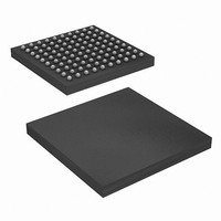
CY7B994V-5BBXCT Cypress Semiconductor Corp, CY7B994V-5BBXCT Datasheet - Page 9

CY7B994V-5BBXCT
Manufacturer Part Number
CY7B994V-5BBXCT
Description
IC,Eighteen Distributed-Output Clock Driver,BGA,100PIN,PLASTIC
Manufacturer
Cypress Semiconductor Corp
Series
RoboClock™r
Type
Clock Buffer, Fanout Distributionr
Datasheet
1.CY7B993V-2AXC.pdf
(18 pages)
Specifications of CY7B994V-5BBXCT
Pll
Yes
Input
LVPECL, LVTTL
Output
LVTTL
Number Of Circuits
1
Ratio - Input:output
4:18
Differential - Input:output
No/No
Frequency - Max
200MHz
Divider/multiplier
Yes/Yes
Voltage - Supply
2.97 V ~ 3.63 V
Operating Temperature
0°C ~ 70°C
Mounting Type
Surface Mount
Package / Case
100-LBGA
Frequency-max
200MHz
Lead Free Status / RoHS Status
Lead free / RoHS Compliant
Available stocks
Company
Part Number
Manufacturer
Quantity
Price
Company:
Part Number:
CY7B994V-5BBXCT
Manufacturer:
Cypress Semiconductor Corp
Quantity:
10 000
INV3 Pin Function
Bank3 has signal invert capability. The four outputs of Bank3 act
as two pairs of complementary outputs when the INV3 pin is
driven LOW. In complementary output mode, 3QA0 and 3QB0
are non-inverting; 3QA1and 3QB1 are inverting outputs. All four
outputs are inverted when the INV3 pin is driven HIGH. When
the INV3 pin is left in MID, the outputs do not invert. Inversion of
the outputs are independent of the skew and divide functions.
Therefore, clock outputs of Bank3 can be inverted, divided, and
skewed at the same time.
Lock Detect Output Description
The LOCK detect output indicates the lock condition of the
integrated PLL. Lock detection is accomplished by comparing
the phase difference between the reference and feedback
inputs. Phase error is declared when the phase difference
between the two inputs is greater than the specified device
propagation delay limit (t
When in the locked state, after four or more consecutive
feedback clock cycles with phase-errors, the LOCK output is
forced LOW to indicate out-of-lock state.
When in the out-of-lock state, 32 consecutive phase-errorless
feedback clock cycles are required to allow the LOCK output to
indicate lock condition (LOCK = HIGH).
If the feedback clock is removed after LOCK has gone HIGH, a
“Watchdog” circuit is implemented to indicate the out-of-lock
condition after a time-out period by deasserting LOCK LOW. This
time out period is based upon a divided down reference clock.
This assumes that there is activity on the selected REF input. If
there is no activity on the selected REF input then the LOCK
detect pin may not accurately reflect the state of the internal PLL.
Factory Test Mode Description
The device enters factory test mode when the OUTPUT_MODE
is driven to MID. In factory test mode, the device operates with
its internal PLL disconnected; input level supplied to the
reference input is used in place of the PLL output. In TEST mode
the selected FB input(s) must be tied LOW. All functions of the
device are still operational in factory test mode except the
internal PLL and output bank disables. The OUTPUT_MODE
input is designed to be a static input. Dynamically toggling this
input from LOW to HIGH may temporarily cause the device to go
into factory test mode (when passing through the MID state).
Factory Test Reset
When in factory test mode (OUTPUT_MODE = MID), the device
can be reset to a deterministic state by driving the DIS4 input
Document #: 38-07127 Rev. *I
PD
).
HIGH. When the DIS4 input is driven HIGH in factory test mode,
all clock outputs go to High Z; after the selected reference clock
pin has five positive transitions, all the internal finite state
machines (FSM) are set to a deterministic state. The determin-
istic state of the state machines depend on the configurations of
the divide selects, skew selects, and frequency select input. All
clock outputs stay in high impedance mode and all FSMs stay in
the deterministic state until DIS4 is deasserted. When DIS4 is
deasserted (with OUTPUT_MODE still at MID), the device
re-enters factory test mode.
Safe Operating Zone
Figure 4
does not exceed its allowable maximum junction temperature of
150 °C.
operate at 185 MHz (with 25 pF load and no air flow) or 200 MHz
(with 10 pF load and no air flow) at various ambient tempera-
tures. At the limit line, all other outputs are configured to
divide-by-two (i.e., operating at 92.5 MHz) or lower frequencies.
The device operates below maximum allowable junction temper-
ature of 150 °C when its configuration (with the specified
constraints) falls within the shaded region (safe operating zone).
Figure 4
that can operate at 200 MHz is 6; and at 70 °C, the maximum
number of outputs that can operate at 185 MHz is 16 (with 25 pF
load and 0-m/s air flow).
Figure 4. Typical Safe Operating Zone
100
Figure 4
95
90
85
80
75
70
65
60
55
50
illustrates the operating condition at which the device
shows that at 85 °C, the maximum number of outputs
2
Num ber of Outputs at 185 MHz
shows the maximum number of outputs that can
Typical Safe Operating Zone
(25-pF Load, 0-m /s air flow )
4
Safe Operating Zone
6
CY7B993V, CY7B994V
8
10
12
14
RoboClock
16
18
Page 9 of 18
[+] Feedback


