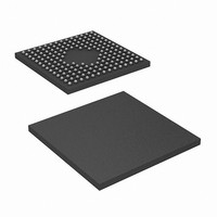
CY7C09579V-83BBC Cypress Semiconductor Corp, CY7C09579V-83BBC Datasheet - Page 9

CY7C09579V-83BBC
Manufacturer Part Number
CY7C09579V-83BBC
Description
IC,SYNC SRAM,32KX36,CMOS,BGA,172PIN,PLASTIC
Manufacturer
Cypress Semiconductor Corp
Datasheet
1.CY7C09579V-100AXC.pdf
(32 pages)
Specifications of CY7C09579V-83BBC
Format - Memory
RAM
Memory Type
SRAM - Dual Port, Synchronous
Memory Size
1.152M (32K x 36)
Speed
83MHz
Interface
Parallel
Voltage - Supply
3 V ~ 3.6 V
Operating Temperature
0°C ~ 70°C
Package / Case
172-LFBGA
Lead Free Status / RoHS Status
Contains lead / RoHS compliant by exemption
Available stocks
Company
Part Number
Manufacturer
Quantity
Price
Company:
Part Number:
CY7C09579V-83BBC
Manufacturer:
Cypress Semiconductor Corp
Quantity:
10 000
Part Number:
CY7C09579V-83BBC
Manufacturer:
CYPRESS/赛普拉斯
Quantity:
20 000
Switching Characteristics
Document Number: 38-06054 Rev. *E
f
f
t
t
t
t
t
t
t
t
t
t
t
t
t
t
t
t
t
t
t
t
t
t
t
t
t
t
t
t
t
t
t
t
t
t
t
t
Notes
MAX1
MAX2
CYC1
CYC2
CH1
CL1
CH2
CL2
R
F
SA
HA
SB
HB
SC
HC
SW
HW
SD
HD
SAD
HAD
SCN
HCN
SRST
HRST
OE
OLZ
OHZ
CD1
CD2
CA1
CA2
DC
CKHZ
CKLZ
CWDD
CCS
10. This parameter is guaranteed by design, but it is not production tested.
11. Test conditions used are Load 2.
Port to Port Delays
Parameter
[10, 11]
[10, 11]
[10, 11]
[10, 11]
f
f
Clock Cycle Time - Flow-Through
Clock Cycle Time - Pipelined
Clock HIGH Time - Flow-Through
Clock LOW Time - Flow-Through
Clock HIGH Time - Pipelined
Clock LOW Time - Pipelined
Clock Rise Time
Clock Fall Time
Address Set-Up Time
Address Hold Time
Byte Select Set-Up Time
Byte Select Hold Time
Chip Enable Set-Up Time
Chip Enable Hold Time
R/W Set-Up Time
R/W Hold Time
Input Data Set-Up Time
Input Data Hold Time
ADS Set-Up Time
ADS Hold Time
CNTEN Set-Up Time
CNTEN Hold Time
CNTRST Set-Up Time
CNTRST Hold Time
Output Enable to Data Valid
OE to Low Z
OE to High Z
Clock to Data Valid - Flow-Through
Clock to Data Valid - Pipelined
Clock to Counter Address Valid -
Flow-Through
Clock to Counter Address Valid - Pipelined
Data Output Hold After Clock HIGH
Clock HIGH to Output High Z
Clock HIGH to Output Low Z
Write Port Clock HIGH to Read Data Delay
Clock to Clock Set-Up Time
Max
Max
Flow-Through
Pipelined
Description
(Over the Operating Range)
Min
6.5
6.5
3.5
0.5
3.5
0.5
3.5
0.5
3.5
0.5
3.5
0.5
3.5
0.5
3.5
0.5
3.5
0.5
15
10
–
–
4
4
–
–
–
2
1
–
–
–
–
2
2
2
–
–
–100
CY7C09569V/CY7C09579V
Max
12.5
12.5
100
67
30
–
–
–
–
–
–
3
3
–
–
–
–
–
–
–
–
–
–
–
–
–
–
–
–
8
–
7
5
9
–
6
–
9
Min
7.5
7.5
0.5
0.5
0.5
0.5
0.5
0.5
0.5
0.5
22
12
–
–
5
5
–
–
4
4
4
4
4
4
4
4
–
2
1
–
–
–
–
2
2
2
–
–
–83
Max
CY7C09569V
CY7C09579V
45
83
18
18
10
35
10
–
–
–
–
–
–
3
3
–
–
–
–
–
–
–
–
–
–
–
–
–
–
–
–
9
–
7
6
–
7
–
Page 9 of 32
Unit
MHz
MHz
ns
ns
ns
ns
ns
ns
ns
ns
ns
ns
ns
ns
ns
ns
ns
ns
ns
ns
ns
ns
ns
ns
ns
ns
ns
ns
ns
ns
ns
ns
ns
ns
ns
ns
ns
ns
[+] Feedback


