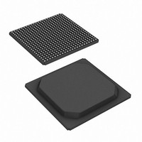
CYD18S72V18-200BGI Cypress Semiconductor Corp, CYD18S72V18-200BGI Datasheet - Page 28

CYD18S72V18-200BGI
Manufacturer Part Number
CYD18S72V18-200BGI
Description
CYD18S72V18-200BGI
Manufacturer
Cypress Semiconductor Corp
Datasheet
1.CYD02S36V18-167BBC.pdf
(52 pages)
Specifications of CYD18S72V18-200BGI
Format - Memory
RAM
Memory Type
SRAM - Dual Port, Synchronous
Memory Size
18M (256K x 72)
Speed
200MHz
Interface
Parallel
Voltage - Supply
1.42 V ~ 1.58 V, 1.7 V ~ 1.9 V
Operating Temperature
-40°C ~ 85°C
Package / Case
484-BGA
Density
18Mb
Access Time (max)
9ns
Sync/async
Synchronous
Architecture
SDR
Clock Freq (max)
77MHz
Operating Supply Voltage (typ)
1.8V
Address Bus
18b
Package Type
BGA
Operating Temp Range
-40C to 85C
Number Of Ports
2
Supply Current
1030mA
Operating Supply Voltage (min)
1.7V
Operating Supply Voltage (max)
1.9V
Operating Temperature Classification
Industrial
Mounting
Surface Mount
Pin Count
484
Word Size
72b
Number Of Words
256K
Lead Free Status / RoHS Status
Lead free / RoHS Compliant
Lead Free Status / RoHS Status
Lead free / RoHS Compliant
Available stocks
Company
Part Number
Manufacturer
Quantity
Price
Company:
Part Number:
CYD18S72V18-200BGI
Manufacturer:
Cypress Semiconductor Corp
Quantity:
10 000
Table 15. Master Reset Timing
Table 16. JTAG Timing
Notes
Document Number: 38-06082 Rev. *J
t
t
t
t
t
t
f
t
t
t
t
t
t
t
t
t
t
t
t
.
55. READY is a wired OR capable output with a weak pull-down. For a decreased falling delay, connect a 250- resistor to VSS.
56. Add this propagation delay after t
PUP
RS
RSR
RSF
RDY
CORDY
JTAG
TCYC
TH
TL
TMSS
TMSH
TDIS
TDIH
TDOV
TDOX
JXZ
JZX
JZX
Parameter
Parameter
[55]
[56]
Power-up time
Master reset pulse width
Master reset recovery time
Master reset to outputs inactive/Hi Z
Master reset release to port ready
C rise to port ready
JTAG TAP controller frequency
TCK cycle time
TCK high time
TCK low time
TMS setup to TCK rise
TMS hold to TCK rise
TDI setup to TCK rise
TDI hold to TCK rise
TCK low to TDO valid
TCK low to TDO invalid
TCK low to TDO high Z
TCK low to TDO active
TCK low to TDO active
RDY
Description
Description
for all Master Reset Operations
Min
Min
50
20
20
10
10
10
10
1
5
5
–
–
–
–
–
0
–
–
–
–200
–200
9.5
1024
Max
Max
10
15
15
15
15
20
–
–
–
–
–
–
–
–
–
–
–
[47]
Min
Min
50
20
20
10
10
10
10
1
5
5
–
–
–
–
–
0
–
–
–
–167
–167
11
1024
Max
Max
18
20
10
15
15
15
–
–
–
–
–
–
–
–
–
–
–
[47]
Min
Min
50
20
20
10
10
10
10
1
5
5
–
–
–
–
–
0
–
–
–
–133
–133
22.50
13
1024
Max
Max
20
10
15
15
15
–
–
–
–
–
–
–
–
–
–
–
[47]
Page 28 of 52
FullFlex
cycles
cycles
cycles
Unit
Unit
MHz
ms
ns
ns
ns
ns
ns
ns
ns
ns
ns
ns
ns
ns
ns
ns
[+] Feedback


