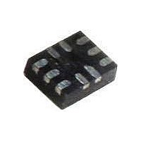
DG2722DN-T1-E4 Vishay, DG2722DN-T1-E4 Datasheet - Page 6

DG2722DN-T1-E4
Manufacturer Part Number
DG2722DN-T1-E4
Description
2 Port,USB 2.0 High Speed Switch,DPDT AS
Manufacturer
Vishay
Type
Analog Switchr
Datasheet
1.DG2722DN-T1-E4.pdf
(8 pages)
Specifications of DG2722DN-T1-E4
Function
USB Switch
Circuit
2 x DPDT
On-state Resistance
8 Ohm
Voltage Supply Source
Single Supply
Voltage - Supply, Single/dual (±)
2.6 V ~ 4.3 V
Current - Supply
2µA
Operating Temperature
-40°C ~ 85°C
Mounting Type
Surface Mount
Package / Case
10-UQFN, 10-µQFN
Number Of Switches
Single
Switch Configuration
DPDT
On Resistance (max)
8 Ohms
On Time (max)
30 ns
Off Time (max)
25 ns
Off Isolation (typ)
- 30 dB
Bandwidth
900 MHz
Supply Voltage (max)
5 V
Supply Voltage (min)
- 0.3 V
Supply Current
2 uA
Maximum Power Dissipation
208 mW
Maximum Operating Temperature
+ 85 C
Mounting Style
SMD/SMT
Description/function
Analog Switch
Minimum Operating Temperature
- 40 C
Off State Leakage Current (max)
100 nA
Switch Current (typ)
+/- 250 mA
Package
10Mini QFN
Maximum Data Rate
480 Mbps
Maximum On Resistance
8@3V Ohm
Maximum Low Level Output Current
250 mA
Number Of Channels Per Chip
1
Maximum Turn-off Time
25@3V ns
Maximum Turn-on Time
30@3V ns
Switch Architecture
DPDT
Power Supply Type
Single
Lead Free Status / RoHS Status
Lead free / RoHS Compliant
Lead Free Status / RoHS Status
Lead free / RoHS Compliant
Other names
DG2722DN-T1-E4TR
Available stocks
Company
Part Number
Manufacturer
Quantity
Price
Company:
Part Number:
DG2722DN-T1-E4
Manufacturer:
Vishay/Siliconix
Quantity:
41 950
Company:
Part Number:
DG2722DN-T1-E4
Manufacturer:
Vishay
Quantity:
700
Part Number:
DG2722DN-T1-E4
Manufacturer:
VISHAY/威世
Quantity:
20 000
DG2722
Vishay Siliconix
TEST CIRCUITS
www.vishay.com
6
V
V
Logic
Input
HSD1±
HSD2±
Switch
V
Input
gen
+
HSD1±
HSD2±
V
IN
C
C
HSD1±
or HSD2±
S
L
L
S
GND
= 0 - V+
(includes fixture and stray capacitance)
(includes fixture and stray capacitance)
R
gen
0 V
V
GND
V+
V+
OUT
OE
V+
V+
=
OE
D±
D±
HSD1±
or HSD2±
OE
D±
(
R
L
+
R
GND
L
V+
V+
R
Switch Output
ON
R
50
R
50 Ω
L
)
Ω
L
Figure 2. Break-Before-Make Interval
S
D±
Figure 3. Charge Injection
Figure 1. Switching Time
C
35 pF
L
C
35 pF
L
V
OUT
V
O
C
L
V
= 1 nF
OUT
HSD1± = HSD2±
Logic
Input
Switch
Output
Switch
Output
Logic
Input
0 V
V
V
V
V
OUT
INH
INL
O
IN
Logic "1" = Switch on
Logic input waveforms inverted for switches that have
the opposite logic sense.
V
V
0 V
INH
INL
IN depends on switch configuration: input polarity
determined by sense of switch.
On
90 %
t
t
D
ON
V
Q =
OUT
50 %
S11-0177-Rev. C, 07-Feb-11
Off
OUT
Document Number: 68379
x C
L
t
D
t
t
r
f
0.9 x V
t
On
OFF
t
t
r
f
<
<
< 5 ns
< 5 ns
5 ns
5 ns
OUT


