DG3157BDN-T1-E4 Vishay, DG3157BDN-T1-E4 Datasheet
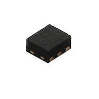
LOW VOLTAGE, SPDT AS

DG3157BDN-T1-E4

Manufacturer Part Number
DG3157BDN-T1-E4
Description
LOW VOLTAGE, SPDT AS
Manufacturer
Vishay
Datasheet

Specifications of DG3157BDN-T1-E4

Function
Switch
Circuit
1 x SPDT
On-state Resistance
15 Ohm
Voltage Supply Source
Single Supply
Voltage - Supply, Single/dual (±)
1.8 V ~ 5.5 V
Current - Supply
1µA
Operating Temperature
-40°C ~ 85°C
Mounting Type
Surface Mount
Package / Case
6-UQFN, 6-µQFN
Number Of Switches
Single
Switch Configuration
SPDT
On Resistance (max)
50 Ohms
Off Isolation (typ)
- 57 dB
Bandwidth
300 MHz
Supply Voltage (max)
6 V
Supply Voltage (min)
- 0.3 V
Maximum Power Dissipation
160 mW
Maximum Operating Temperature
+ 85 C
Mounting Style
SMD/SMT
Minimum Operating Temperature
- 40 C
Switch Current (typ)
+/- 50 mA
Lead Free Status / RoHS Status
Lead free / RoHS Compliant
Lead Free Status / RoHS Status
Lead free / RoHS Compliant
Other names
DG3157BDN-T1-E4TR

Available stocks

Company
Part Number
Manufacturer
Quantity
Price
Part Number:
DG3157BDN-T1-E4
Manufacturer:
Infineon
Quantity:
50
Part Number:
DG3157BDN-T1-E4
Manufacturer:
VISHAY/威世
Quantity:
20 000
DESCRIPTION
The DG3157A, DG3157B are high-speed single-pole
double-throw, low voltage switch. Using sub-micro CMOS
technology, the DG3157A, DG3157B achieves low on-
resistance and negligible propagation delay. The DG3157A,
DG3157B can handle both analog and digital signals and
permits signals with amplitudes of up to V
transmitted in either direction. Select pin of control logic input
can be over the V+. When the select pin is low, B
connected to the output A pin. When the select pin is high,
B
have a high-impedance state with respect to the output A pin.
Break before make is guaranteed. The DG3157A has an
internal pull down resistor on the control pin S, while the
DG3157B does not.
FUNCTIONAL BLOCK DIAGRAM AND PIN CONFIGURATION
* Pb containing terminations are not RoHS compliant, exemptions may apply.
Low Voltage, 300-MHz - 3 dB Bandwidth, SPDT Analog Switch with
Document Number: 68628
S-81944-Rev. C, 25-Aug-08
1
is connected to the output A pin. The path that is open will
GND
GND
B
B
B
B
1
0
1
0
2
3
1
2
3
1
Device Marking: D
Device Marking: E
miniQFN-6
DG3157B
miniQFN-6
DG3157A
Top View
Top View
(2:1 Multiplexer/Demultiplexer Bus Switch)
6
5
4
6
5
4
S
V+
A
Power Down Protection
S
V+
A
CC
to be
0
is
FEATURES
• Ultra small miniQFN6 package of
• Wide operation voltage range: 1.8 V to 5.5 V
• Useful in both analog and digital signal
• 300 MHz - 3 dB bandwidth
• Power down safe design
• Low voltage logic threshold:
• Minimal propagation delay
• Break-before-make switching
• Zero bounce in flow-through mode
• > 300 mA latch up current per JESD78
• > 8 kV ESD/HBM
• DG3157A version has internal pull down resistor on
- 40 °C to 85 °C
TRUTH TABLE
ORDERING INFORMATION
Temp. Range
1 mm x 1.2 mm
switching
V
control pin S
th
(high) = 1.2 V at V+ = 3.3 V
Logic Input (S)
0
1
DG3157A, DG3157B
miniQFN-6
Package
Vishay Siliconix
B
B
0
1
Connected to A
Connected to A
Function
DG3157ADN-T1-E4
DG3157BDN-T1-E4
Part Number
www.vishay.com
RoHS*
COMPLIANT
Available
Pb-free
1

Related parts for DG3157BDN-T1-E4

DG3157BDN-T1-E4 Summary of contents

Page 1

... JESD78 • > ESD/HBM • DG3157A version has internal pull down resistor on control pin S TRUTH TABLE ORDERING INFORMATION Temp. Range - 40 ° ° DG3157A, DG3157B Vishay Siliconix Logic Input (S) Function B Connected Connected Package Part Number DG3157ADN-T1-E4 miniQFN-6 DG3157BDN-T1-E4 www.vishay.com Pb-free Available RoHS* COMPLIANT 1 ...

Page 2

... DG3157A, DG3157B Vishay Siliconix ABSOLUTE MAXIMUM RATINGS Parameter Reference V+ to GND Continuous Current (Any terminal) Peak Current (Pulsed duty cycle) Storage Temperature b Power Dissipation (Packages) Notes: a. Signals exceeding V+ will be clamped by internal diodes. Limit forward diode current to maximum current ratings. b. All leads welded or soldered to PC board. ...

Page 3

... V+ = 3 4 GEN Ω 3.3 V GEN = 50 Ω MHz Ω 600 Ω, 0.5 Vp 600 kHz IO DG3157A, DG3157B Vishay Siliconix Limits - 40 ° ° Temp. Min. Typ. Max. Full 1.65 5.5 Room 1 Full 10 Full 1.5 Full 0.8 Full 0.4 Full 0.3 Room ...

Page 4

... DG3157A, DG3157B Vishay Siliconix LOGIC DIAGRAM Positive Logic LOADING AND WAVEFORMS From Output Under Test Switch Input Output Propagation Delay T imes Notes: • C includes probe and jig capacitance. L • Waveform 1 is for an output with internal conditions such that the output is low except when disabled by the output control. ...

Page 5

... Supply Voltage ON A Document Number: 68628 S-81944-Rev. C, 25-Aug- °C, unless otherwise noted ° 4 Loss OIRR - 100 100k 100 M Frequency (Hz) Insertion Loss, Off-Isolation, Crosstalk vs. Frequency DG3157A, DG3157B Vishay Siliconix 2.0 1.5 1.0 0.5 0 Supply Voltage (V) Switching Threshold vs. Supply Voltage TALK Ω www.vishay.com 5 ...

Page 6

... Figure 6. Off-Isolation Vishay Siliconix maintains worldwide manufacturing capability. Products may be manufactured at one of several qualified locations. Reliability data for Silicon Tech- nology and Package Reliability represent a composite of all qualified locations. For related documents such as package/tape drawings, part marking, and reliability data, see http://www.vishay.com/ppg?68628. ...

Page 7

... Vishay product could result in personal injury or death. Customers using or selling Vishay products not expressly indicated for use in such applications their own risk and agree to fully indemnify and hold Vishay and its distributors harmless from and against any and all claims, liabilities, expenses and damages arising or resulting in connection with such use or sale, including attorneys fees, even if such claim alleges that Vishay or its distributor was negligent regarding the design or manufacture of the part ...

Related keywords