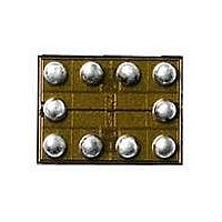
DG3516DB-T5-E1 Vishay, DG3516DB-T5-E1 Datasheet

DG3516DB-T5-E1
Specifications of DG3516DB-T5-E1
Available stocks
Related parts for DG3516DB-T5-E1
DG3516DB-T5-E1 Summary of contents
Page 1
... ORDERING INFORMATION Temp Range DG3517 GND V+ Top View - ° COM DG3516/DG3517 Vishay Siliconix ON ® Package Logic NC1 and NC2 NO1 and NO2 OFF Package Part Number MICRO FOOT: 10 Bump DG3516DB-T5- 0.5 mm Pitch, DG3517DB-T5-E1 238 µm Bump Height) www.vishay.com RoHS COMPLIANT OFF ON 1 ...
Page 2
... DG3516/DG3517 Vishay Siliconix ABSOLUTE MAXIMUM RATINGS Parameter Reference V+ to GND a IN, COM, NC, NO Continuous Current (NO, NC, COM) Peak Current (Pulsed duty cycle) Storage Temperature b Package Solder Reflow Conditions ESD per Method 3015.7 c Power Dissipation (Packages) Notes: a. Signals on NC, NO, or COM or IN exceeding V+ will be clamped by internal diodes. Limit forward diode current to maximum current ratings. ...
Page 3
... 2 1 300 Ω OFF nF 2 INJ L GEN GEN MHz MHz = 50 Ω MHz TALK MHz V MHz DG3516/DG3517 Vishay Siliconix Limits - ° Temp Min Typ Max Room 21 Full Room 15 Full Full Ω Room 1 Room - 74 Room - 54 Room - 76 Room - 56 Room 12 Room 12 Room 40 Room 40 Room Full www ...
Page 4
... DG3516/DG3517 Vishay Siliconix SPECIFICATIONS ( Parameter Symbol Analog Switch Analog Signal Range On-Resistance Flatness ON Flatness On-Resistance Δr DS(on) d Match Between Channels I NO(off) I NC(off) Switch Off Leakage Current I COM(off) I Channel-On Leakage Current COM(on) Digital Control d V Input High Voltage V Input Low Voltage Input Capacitance ...
Page 5
... DG3516/DG3517 Vishay Siliconix 4 °C 25 ° ° Analog Voltage (V) COM r vs. Analog Voltage and Temperature 3 100 100 Input Switching Frequency (Hz) Supply Current vs ...
Page 6
... DG3516/DG3517 Vishay Siliconix TYPICAL CHARACTERISTICS 25 °C, unless otherwise noted 10000 V+ = 3.0 V 1000 I COM(off) I COM(on) 100 Temperature (°C) Leakage Current vs. Temperature 2 4 2.7 V OFF Temperature (°C) Switching Time vs. Temperature 2.00 1.75 1.50 1.25 1.00 0.75 0.50 0.25 0. Supply Voltage (V) Switching Threshold vs. Supply Voltage www ...
Page 7
... Ω 300 Switch 0 V Output Figure 2. Break-Before-Make Interval COM V OUT Figure 3. Charge Injection DG3516/DG3517 Vishay Siliconix V INH INL Logic “1” = Switch On Logic input waveforms inverted for switches that have the opposite logic sense. INH INL ΔV OUT V OUT IN On Off Q = Δ ...
Page 8
... DG3516/DG3517 Vishay Siliconix TEST CIRCUITS Analyzer 0 V, 2.4 V www.vishay.com COM COM R L GND V COM Off Isolation = 20 log Figure 4. Off-Isolation COM GND Figure 5. Channel Off/On Capacitance Meter HP4192A Impedance Analyzer or Equivalent MHz Document Number: 73404 S-70853-Rev. C, 30-Apr-07 ...
Page 9
... Use millimeters as the primary measurement. Vishay Siliconix maintains worldwide manufacturing capability. Products may be manufactured at one of several qualified locations. Reliability data for Silicon Tech- nology and Package Reliability represent a composite of all qualified locations. For related documents such as package/tape drawings, part marking, and reliability data, see http://www ...
Page 10
... Vishay disclaims any and all liability arising out of the use or application of any product described herein or of any information provided herein to the maximum extent permitted by law. The product specifications do not expand or otherwise modify Vishay’ ...


