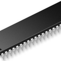
DSPIC33FJ16GS404-I/TL Microchip Technology, DSPIC33FJ16GS404-I/TL Datasheet - Page 195

DSPIC33FJ16GS404-I/TL
Manufacturer Part Number
DSPIC33FJ16GS404-I/TL
Description
16 Bit MCU/DSP 40MIPS 16 KB FLASH 2KB RAM SMPS 44 TLA 6x6x0.9 Mm TUBE
Manufacturer
Microchip Technology
Series
dsPIC™ 33Fr
Datasheet
1.DSPIC33FJ06GS101-ISO.pdf
(346 pages)
Specifications of DSPIC33FJ16GS404-I/TL
Core Processor
dsPIC
Core Size
16-Bit
Speed
40 MIPs
Connectivity
I²C, IrDA, LIN, SPI, UART/USART
Peripherals
Brown-out Detect/Reset, POR, PWM, WDT
Number Of I /o
35
Program Memory Size
16KB (16K x 8)
Program Memory Type
FLASH
Ram Size
2K x 8
Voltage - Supply (vcc/vdd)
3 V ~ 3.6 V
Data Converters
A/D 8x10b
Oscillator Type
Internal
Operating Temperature
-40°C ~ 85°C
Package / Case
*
Processor Series
dsPIC33FJ
Core
dsPIC
Data Bus Width
16 bit
Data Ram Size
2 KB
Interface Type
I2C, SPI, UART
Maximum Clock Frequency
40 MHz
Number Of Programmable I/os
35
Operating Supply Voltage
3 V to 3.6 V
Maximum Operating Temperature
+ 85 C
Mounting Style
Through Hole
Development Tools By Supplier
DM240001, DM240002
Lead Free Status / RoHS Status
Lead free / RoHS Compliant
Eeprom Size
-
Lead Free Status / Rohs Status
Details
- Current page: 195 of 346
- Download datasheet (6Mb)
14.0
The output compare module can select either Timer2 or
Timer3 for its time base. The module compares the
value of the timer with the value of one or two Compare
registers depending on the operating mode selected.
FIGURE 14-1:
© 2009 Microchip Technology Inc.
Note:
OUTPUT COMPARE
Note: An ‘x’ in a signal, register or bit name denotes the number of the output compare channels.
This data sheet summarizes the features
of
dsPIC33FJ16GSX02/X04
devices. It is not intended to be a
comprehensive reference source.
complement the information in this data
sheet, refer to the “dsPIC33F Family
Reference Manual”, Section 13. “Output
Compare” (DS70209), which is available
on
(www.microchip.com).
dsPIC33FJ06GS101/X02 and dsPIC33FJ16GSX02/X04
the
the
dsPIC33FJ06GS101/X02
OUTPUT COMPARE MODULE BLOCK DIAGRAM
16
TMR2
Comparator
Microchip
0
OCxRS
OCxR
TMR3
1
16
OCTSEL
families
web
and
Rollover Rollover
site
Preliminary
TMR2
To
of
0
TMR3
1
The state of the output pin changes when the timer
value matches the Compare register value. The output
compare module generates either a single output
pulse, or a sequence of output pulses, by changing the
state of the output pin on the compare match events.
The output compare module can also generate
interrupts on compare match events.
The output compare module has multiple operating
modes:
• Active-Low One-Shot mode
• Active-High One-Shot mode
• Toggle mode
• Delayed One-Shot mode
• Continuous Pulse mode
• PWM mode without Fault Protection
• PWM mode with Fault Protection
Mode Select
OCM<2:0>
Output
Logic
3
Set Flag bit
OCxIF
R
S
Q
Output Enable
DS70318D-page 193
OCx
OCFA
Related parts for DSPIC33FJ16GS404-I/TL
Image
Part Number
Description
Manufacturer
Datasheet
Request
R

Part Number:
Description:
IC, DSC, 16BIT, 12KB, 40MHZ, 3.6V, DIP28
Manufacturer:
Microchip Technology
Datasheet:

Part Number:
Description:
Manufacturer:
Microchip Technology Inc.
Datasheet:

Part Number:
Description:
Manufacturer:
Microchip Technology Inc.
Datasheet:

Part Number:
Description:
Manufacturer:
Microchip Technology Inc.
Datasheet:

Part Number:
Description:
Manufacturer:
Microchip Technology Inc.
Datasheet:

Part Number:
Description:
Manufacturer:
Microchip Technology Inc.
Datasheet:

Part Number:
Description:
Manufacturer:
Microchip Technology Inc.
Datasheet:

Part Number:
Description:
Manufacturer:
Microchip Technology Inc.
Datasheet:

Part Number:
Description:
Manufacturer:
Microchip Technology Inc.
Datasheet:


