JN5139-001-M/04R1T NXP Semiconductors, JN5139-001-M/04R1T Datasheet
JN5139-001-M/04R1T
Specifications of JN5139-001-M/04R1T
935294017534
JN5139-001-M04
JN5139-001-M04R1T
JN5139-001-M04R1T
Q3424158
Available stocks


Related parts for JN5139-001-M/04R1T


JN5139-001-M/04R1T Summary of contents
Page 1
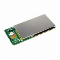
... IEEE802.15.4/ZigBee Module Family Overview Overview The JN5139-xxx-Myy family is a range of surface mount modules that enable users to The JN5139-xxx-Myy family is a range of surface mount modules that enable users to implement systems using IEEE802.15.4, 6LoWPAN, JenNet or ZigBee with minimum implement systems using IEEE802.15.4, 6LoWPAN, JenNet or ZigBee with minimum time to market and at the lowest cost ...
Page 2
... A.4.3 Leader and Trailer A.4.4 Reel Dimensions: A.5 Related Documents A.6 Federal Communication Commission Interference Statement A.6.1 Antennas approved by FCC for use with JN5139 modules A.6.2 High Power Module usage limitation A.6.3 FCC End Product Labelling A.7 European R & TTE Directive 1999/5/EC Statement A ...
Page 3
... Introduction The JN5139-xxx-Myy module family provides designers with a ready made component which allows IEEE802.15.4 [1] wireless applications, using Jennic’s JenNet networking protocol or ZigBee quickly and easily included in product designs. The modules integrate all of the RF components required, removing the need to perform expensive RF design and test. Products can be designed by simply connecting sensors and switches to the module IO pins. The modules use Jennic’ ...
Page 4
... Specifications Most specification parameters for the modules are specified in the chip datasheet - JN-DS- JN5139 Wireless Microcontroller Datasheet, [2]. Where there are differences, the parameters are defined here. VDD=3.0V @ +25°C Typical DC Characteristics Deep sleep current Sleep current Radio transmit current Radio receive current ...
Page 5
... JN5139 Single Chip Wireless Microcontroller The JN5139-xxx-Myy series is constructed around the JN5139 single chip wireless microcontroller, which includes the radio system, a 32-bit RISC CPU, ROM and RAM memory and a range of analogue and digital peripherals. The chip is described fully in JN-DS- JN5139 Wireless Microcontroller Datasheet [2]. ...
Page 6
... SPISSM 13 SPISWP 14 DIO3/SPISEL4 15 Note that the same basic pin configuration applies for all module designs. However, DIO3/SPISEL4 and DIO2/SPISEL3 are not available on the high power modules Figure 1: Pin Configuration (top view) JN-DS-JN5139-xxx-Myy 1v6 ADC3 41 ADC2 40 39 ADC1 COMP1+ 38 COMP1- 37 DIO20/RXD1 36 DIO19/TXD1 ...
Page 7
... RESETN Active low reset 30 SIF_CLK Serial Interface clock / Intelligent peripheral clock © NXP Laboratories UK 2010 JN-DS-JN5139-xxx-Myy 1v6 Alternative Function General Purpose Digital I/O DIO0 General Purpose Digital I/O DIO1 General Purpose Digital I/O DIO2 * General Purpose Digital I/O DIO3* General Purpose Digital I/O DIO4 ...
Page 8
... ADC3 Analogue to Digital input *: These two pins are not connected for High power modules 4.2. Pin Descriptions All pins behave as described in the JN-DS- JN5139 Wireless Microcontroller Datasheet [2], with the exception of the following: 4.2.1 Power Supplies A single power supply pin, VDD is provided. Separate analogue (VSSA) and digital (GND) grounds are provided. ...
Page 9
... Figure 2: Recommended solder reflow profile © NXP Laboratories UK 2010 Min -0.3V -0.3V -0.3V -40ºC 160~190 ºC > 220º C 30~60 20~50 JN-DS-JN5139-xxx-Myy 1v6 Max 3.6V VDD + 0.3V Lower of (VDD + 2V) and 5.5V 150ºC 260ºC 230~Pk. Pk. Temp (235ºC) 10~15 160~270 ...
Page 10
... Operating Conditions Supply VDD Ambient temperature range 10 Min 2.7V -20°C JN-DS-JN5139-xxx-Myy 1v6 Max 3.6V 70°C © NXP Laboratories UK 2010 ...
Page 11
... Appendix A Additional Information A.1 Outline Drawing 30mm 2.54 mm Thickness: 3.5mm © NXP Laboratories UK 2010 18mm J1 Figure 3 JN5139-xxx-M00 Outline Drawing JN-DS-JN5139-xxx-Myy 1v6 1.27 mm 2. ...
Page 12
... Thickness: 3.5mm over can, 10.8mm at SMA connector 12 18mm 9.74mm Figure 4 JN5139-xxx-M01 Outline Drawing JN-DS-JN5139-xxx-Myy 1v6 4.59 mm 1.27 mm 2.54 mm 2.76 mm © NXP Laboratories UK 2010 ...
Page 13
... Thickness: 3.5mm © NXP Laboratories UK 2010 18mm 9.76mm Figure 5 JN5139-xxx-M03 Outline Drawing JN-DS-JN5139-xxx-Myy 1v6 6.58 mm 1.27 mm 2. ...
Page 14
... Thickness: 3.5mm over can, 10.8mm at SMA connector. 14 18mm 7.2mm 2.76 mm Figure 6 JN5139-xxx-M02 Outline Drawing JN-DS-JN5139-xxx-Myy 1v6 4.32 mm 1.27 mm 2.54 mm © NXP Laboratories UK 2010 ...
Page 15
... Thickness: 3.5mm © NXP Laboratories UK 2010 18mm 7.2mm 2.76 mm Figure 7 JN5139-xxx-M04 Outline Drawing JN-DS-JN5139-xxx-Myy 1v6 4.05mm 1. ...
Page 16
... Tracks etc may be placed adjacent to the can, but should not extend past the can towards the antenna end of the module for 20mm from the antenna. 16 Figure 8 Module PCB footprint JN-DS-JN5139-xxx-Myy 1v6 Dimensions in mm © NXP Laboratories UK 2010 ...
Page 17
... Ordering Code Format: JN5139 - XXX - M / Y1Y2 Y3 Y4 Part Number Ordering Code JN5139-001-M00R1T JN5139-001-M/00R1T JN5139-001-M01R1V JN5139-001-M/01R1V JN5139-001-M02R1V JN5139-001-M/02R1V JN5139-001-M03R1T JN5139-001-M/03R1T JN5139-001-M04R1T JN5139-001-M/04R1T JN5139-Z01-M00R1T JN5139-Z01-M/00R1T JN5139-Z01-M01R1V JN5139-Z01-M/01R1V JN5139-Z01-M02R1V JN5139-Z01-M/02R1V JN5139-Z01-M03R1T JN5139-Z01-M/03R1T JN5139-Z01-M04R1T JN5139-Z01-M/04R1T Label line Number Label line 2: FCC ID Number Label line 3: Part Number ...
Page 18
... Ohms/sq Non-conductive Polyester PSA Room ambient JN-DS-JN5139-xxx-Myy 1v6 Cover Tape width (W) 2.0 24.0 3.4 37.5 2.0 24.0 11.2 49.5 2.0 24.0 11.1 49.5 2.0 24.0 3.4 49.5 ±0.1 ± ...
Page 19
... A.4.3 Leader and Trailer 300 MM A.4.4 Reel Dimensions: Module type: JN5139-xxx-M00/03 JN5139-xxx-M01/02/04 © NXP Laboratories UK 2010 330 ±1.0 2.2±0.5 13 ±0.2 330 ±1.0 2.2±0.5 13 ±0.2 JN-DS-JN5139-xxx-Myy 1v6 300 MM Dimensions (min) 100 +0.1 44.5 ±0.3 100 +0.1 56.5 ±0.3 19 ...
Page 20
... IEEE Std 802.15.4-2003 IEEE Standard for Information Technology – Part 15.4 Wireless Medium Access Control (MAC) and Physical Layer (PHY) Specifications for Low-Rate Wireless Personal Area Networks (LR-WPANs) [2] JN-DS- JN5139 Wireless Microcontroller Datasheet [3] JN-RM-2002 802.15.4 Stack API A.6 Federal Communication Commission Interference Statement This equipment has been tested and found to comply with the limits for a Class B digital device, pursuant to Part 15 of the FCC Rules ...
Page 21
... A.6.1 Antennas approved by FCC for use with JN5139 modules Brand 1 Aveslink Technology, Inc 2 Aveslink Technology, Inc 3 Aveslink Technology, Inc 4 Aveslink Technology, Inc 5 Aveslink Technology, Inc 6 Aveslink Technology, Inc 7 Aveslink Technology, Inc 8 Aveslink Technology, Inc 9 Aveslink Technology, Inc 10 Aveslink Technology, Inc 11 Aveslink Technology, Inc ...
Page 22
... A.6.3 FCC End Product Labelling The final ‘end product’ should be labelled in a visible area with the following: “Contains TX FCC ID: TYOJN5139M0, TYOJN5139M3 or TYOJN5139M4 ” to reflect the version of the module being used inside the product. 22 ...
Page 23
... Vertical - bulkhead- flying lead Vertical - swivel Vertical - swivel Vertical - swivel -flying lead Vertical - bulkhead- flying lead Vertical - swivel Vertical - swivel Vertical - right angle Embedded - flying lead Vertical – tilt and swivel JN-DS-JN5139-xxx-Myy 1v6 Gain Connector type 2.9dBi RP-SMA 2.2dBi SMA 1.0dBi SMA 1.5dBi uFL 2 ...
Page 24
... A.9 RoHS Compliance JN5139-xxx-Myy devices meet the requirements of Directive 2002/95/EC of the European Parliament and of the Council on the Restriction of Hazardous Substance (RoHS). The JN5139-xxx-M00, M03 and M04 modules are fully compliant with the Chinese RoHS requirements SJ/T11363- 2006 ...
Page 25
... The functionality of the product is final. The electrical performance specifications are target values and may used as a guide to the final specification. Modules are identified with an R1 suffix, for example JN5139-Z01-M00R1. Jennic reserves the right to make changes to the product specification at anytime without notice. ...
Page 26
... Updated to preliminary status, solder reflow profile and antenna lists added. Increased length of –M02 variants 1.3 Updated part numbering and addition of Industry Canada approvals 1.4 Minor specification updates 1.5 Updated antenna information and other minor specification updates 1.6 References to NXP added and ordering information changed 26 JN-DS-JN5139-xxx-Myy 1v6 © NXP Laboratories UK 2010 ...
Page 27
... For the contact details of your local Jennic office or distributor, refer to the Jennic web site: © NXP Laboratories UK 2010 NXP Laboratories UK Ltd (Formerly Jennic Ltd) Furnival Street Sheffield S1 4QT United Kingdom Tel: +44 (0)114 281 2655 Fax: +44 (0) 114 281 2951 E-mail: info@jennic.com www.nxp.com/jennic JN-DS-JN5139-xxx-Myy 1v6 27 ...