KSZ8001L TR Micrel Inc, KSZ8001L TR Datasheet - Page 6
KSZ8001L TR
Manufacturer Part Number
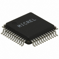
KSZ8001L TR
Description
10/100 BASE-TX/FX Physical Layer Transceiver With LinkMD Cable Diagnostics, Single 3.3V Supply, 48-LQFP,
Manufacturer
Micrel Inc
Type
Transceiverr
Specifications of KSZ8001L TR
Protocol
MII, RMII, SMII
Voltage - Supply
1.8V, 3.3V
Mounting Type
Surface Mount
Package / Case
48-LQFP
Lead Free Status / RoHS Status
Lead free / RoHS Compliant
For Use With
576-1620 - BOARD EVALUATION FOR KSZ8001L
Number Of Drivers/receivers
-
Lead Free Status / Rohs Status
Compliant
Other names
KSZ8001LTR
KSZ8001LTR
KSZ8001LTR


March 2006
Micrel
Pin Description
Pin Number
1
2
3
4
5
6
7
8
9
10
11
12
13
14
15
16
Pin Name
MDIO
MDC
RXD3/
PHYAD1
RXD2/
PHYAD2
RXD1/
RXD[1]/
PHYAD3
RXD0/
RXD[0]/
RX
PHYAD4
VDDIO
GND
RXDV/
CRSDV/
PCS_LPBK
RXC/
SMII_SELE
CT
RXER/
RX_ER/
ISO
GND
VDDC
TXER
TXC/
REFCLK/
CLOCK
TXEN
Type
I/O
I
Ipd/O
Ipd/O
Ipd/O
Ipd/O
Pwr
Gnd
Ipd/O
Ipd/O
Ipd/O
Gnd
Pwr
Ipd
I/O
Ipd
(Note 1)
Pin Function
MII Management (MIIM) Interface: Data I/O
This pin requires an external 4.7K pull-up resistor.
MII Management (MIIM) Interface: Clock Input
This pin is synchronous to the MDIO data line.
MII Mode: Receive Data Output[3]
Configuration Mode: The pull-up/pull-down value is latched as PHYADDR[1]
during reset. See “Strapping Options” section for details.
MII Mode: MII Receive Data Output[2]
Configuration Mode: The pull-up/pull-down value is latched as PHYADDR[2]
during reset. See “Strapping Options” section for details.
MII Mode: Receive Data Output[1]
RMII Mode: Receive Data Output[1]
Configuration Mode: The pull-up/pull-down value is latched as PHYADDR[3]
during reset. See “Strapping Options” section for details.
MII Mode: Receive Data Output[0]
RMII Mode: Receive Data Output[0]
SMII Mode: Receive Data and Control
Configuration Mode: The pull-up/pull-down value is latched as PHYADDR[4]
during reset. See “Strapping Options” section for details.
3.3V digital VDD
Ground
MII Mode: Receive Data Valid Output /
RMII Mode: Carrier Sense/Receive Data Valid /
Configuration Mode: The pull-up/pull-down value is latched as pcs_lpbk
during reset. See “Strapping Options” section for details.
MII Receive Clock Output
Operating at:
25 MHz = 100 Mbps
2.5 MHz = 10 Mbps
Configuration Mode: The pull-up/pull-down value is latched as SMII during
reset. See “Strapping Options” section for details.
MII Mode: Receive Error Output /
RMII Mode: Receive Error /
Configuration Mode: The pull-up/pull-down value is latched as ISOLATE
during reset. See “Strapping Options” section for details.
Ground
1.8V digital core VDD
(See “Circuit Design Reference for Power Supply” section for details)
MII Transmit Error Input
MII Mode: MII Transmit Clock Output /
RMII Mode: 50 MHz Reference Clock Input /
SMII Mode: 125 MHz Synchronization Clock Input
MII Transmit Enable Input
VDD output
VDD input
6
:
:
2
2
2
KSZ8001L / KSZ8001SL
KSZ8001S
/
/
/
3
3
/
/
2
4
/
/
Revision 1.03
KSZ8001
Related parts for KSZ8001L TR
Image
Part Number
Description
Manufacturer
Datasheet
Request
R

Part Number:
Description:
Manufacturer:
Micrel Inc
Datasheet:
Part Number:
Description:
Manufacturer:
Micrel Inc
Datasheet:
Part Number:
Description:
Manufacturer:
Micrel Inc
Datasheet:
Part Number:
Description:
Manufacturer:
Micrel Inc
Datasheet:
Part Number:
Description:
Manufacturer:
Micrel Inc
Datasheet:
Part Number:
Description:
Manufacturer:
Micrel Inc
Datasheet:
Part Number:
Description:
Manufacturer:
Micrel Inc
Datasheet:
Part Number:
Description:
Manufacturer:
Micrel Inc
Datasheet:
Part Number:
Description:
Manufacturer:
Micrel Inc
Datasheet:
Part Number:
Description:
Manufacturer:
Micrel Inc
Datasheet:
Part Number:
Description:
Manufacturer:
Micrel Inc
Datasheet:
Part Number:
Description:
Manufacturer:
Micrel Inc
Datasheet:
Part Number:
Description:
Manufacturer:
Micrel Inc
Datasheet:
Part Number:
Description:
Manufacturer:
Micrel Inc
Datasheet: