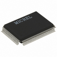
KSZ8995MAI Micrel Inc, KSZ8995MAI Datasheet - Page 76

KSZ8995MAI
Manufacturer Part Number
KSZ8995MAI
Description
IC,Telecom Switching Circuit,CMOS,QFP,128PIN,PLASTIC
Manufacturer
Micrel Inc
Specifications of KSZ8995MAI
Applications
*
Mounting Type
Surface Mount
Package / Case
128-MQFP, 128-PQFP
Number Of Primary Switch Ports
5
Internal Memory Buffer Size
64
Operating Supply Voltage (typ)
Not RequiredV
Fiber Support
Yes
Integrated Led Drivers
Yes
Data Rate
100Mbps
Phy/transceiver Interface
MII/SNI
Power Supply Type
Analog/Digital
Package Type
PQFP
Data Rate (typ)
10/100Mbps
Vlan Support
Yes
Operating Temperature (max)
85C
Operating Temperature (min)
-40C
Pin Count
128
Mounting
Surface Mount
Jtag Support
No
Operating Supply Voltage (max)
Not RequiredV
Operating Supply Voltage (min)
Not RequiredV
Operating Temperature Classification
Industrial
Lead Free Status / RoHS Status
Lead free / RoHS Compliant
For Use With
576-1607 - BOARD EVAL EXPERIMENT KSZ8995MA
Lead Free Status / Rohs Status
Compliant
Other names
576-2126
KSZ8995MAI
KSZ8995MAI
Available stocks
Company
Part Number
Manufacturer
Quantity
Price
Company:
Part Number:
KSZ8995MAI
Manufacturer:
TI
Quantity:
1 700
Company:
Part Number:
KSZ8995MAI
Manufacturer:
MICREL
Quantity:
5
Part Number:
KSZ8995MAI
Manufacturer:
MICREL/麦瑞
Quantity:
20 000
Semptember 2008
Reset Circuit Diagram
Micrel recommends the following discrete reset circuit as shown in Figure 22 when powering up the KS8895MA device.
For the application where the reset circuit signal comes from another device (e.g., CPU, FPGA, etc), we recommend
the reset circuit as shown in Figure 23.
At power-on-reset, R, C, and D1 provide the necessary ramp rise time to reset the Micrel device. The reset out from
CPU/FPGA provides warm reset after power up. It is also recommended to power up the VDD core voltage earlier than
VDDIO voltage. At worst case, the both VDD core and VDDIO voltages should come up at the same time.
Figure 23. Recommended Circuit for Interfacing with CPU/FPGA Reset
KS8995MA
RST
Figure 22. Recommended Reset Circuit
KS8995MA
D1
D1: 1N4148
RST
10µF
VCC
C
76
D1
R
10k
D2
10µF
VCC
D1, D2: 1N4148
C
R
10k
RST_OUT_n
CPU/FPGA
M9999-091508


