SI824XCLASSD-KIT Silicon Laboratories Inc, SI824XCLASSD-KIT Datasheet - Page 18
SI824XCLASSD-KIT
Manufacturer Part Number
SI824XCLASSD-KIT
Description
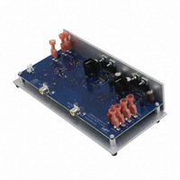
BOARD EVAL FOR SI824X
Manufacturer
Silicon Laboratories Inc
Datasheet
1.SI8241CB-B-IS1.pdf
(30 pages)
Specifications of SI824XCLASSD-KIT
New! Us2012 Catalog Page
Class-D Audio Driver_Precision Clock ICs
Board Type
Fully Populated
Amplifier Type
Class D
Output Type
2-Channel (Stereo)
Max Output Power X Channels @ Load
120W x 2 @ 8 Ohm
Utilized Ic / Part
Si824x
Description/function
Audio Amplifiers
Operating Supply Voltage
12 V
Output Power
30 W to 1000 W
Product
Audio Development Tools
Supply Current
500 mA
For Use With/related Products
Si824x
Lead Free Status / RoHS Status
Lead free / RoHS Compliant
Voltage - Supply
-
Operating Temperature
-
Lead Free Status / RoHS Status
Lead free / RoHS Compliant
Other names
336-2002


Si824x
3.4. Power Supply Connections
Isolation requirements mandate individual supplies for VDDI, VDDA, and VDDB. The decoupling caps for these
supplies must be placed as close to the VDD and GND pins of the Si824x as possible. The optimum values for
these capacitors depend on load current and the distance between the chip and the regulator that powers it. Low
effective series resistance (ESR) capacitors, such as Tantalum, are recommended.
3.5. Power Dissipation Considerations
Proper system design must assure that the Si824x operates within safe thermal limits across the entire load range.
The Si824x total power dissipation is the sum of the power dissipated by bias supply current, internal switching
losses, and power delivered to the load. Equation 1 shows total Si824x power dissipation. In a non-overlapping
system, such as a high-side/low-side driver, n = 1.
The maximum power dissipation allowable for the Si824x is a function of the package thermal resistance, ambient
temperature, and maximum allowable junction temperature, as shown in Equation 2:
Substituting values for P
dissipation of 1.19 W. Maximum allowable load is found by substituting this limit and the appropriate datasheet
values from Table 1 on page 5 into Equation 1 and simplifying. The result is Equation 3 (0.5 A driver) and
Equation 4 (4.0 A driver), both of which assume VDDI = 5 V and VDDA = VDDB = 18 V.
18
P
where:
P
I
I
C
V
V
F is the switching frequency (Hz)
n is the overlap constant (max value = 2)
DDI
QOUT
D
D
DDI
DDO
int
Dmax
is the total Si824x device power dissipation (W)
=
is the internal parasitic capacitance (75 pF for the 0.5 A driver and 370 pF for the 4.0 A driver)
is the input-side maximum bias current (3 mA)
is the input-side VDD supply voltage (4.5 to 5.5 V)
V
is the driver-side supply voltage (10 to 24 V)
P
where:
P
T
T
ja = Si824x junction-to-air thermal resistance (105 °C/W)
F = Si824x switching frequency (Hz)
is the driver die maximum bias current (2.5 mA)
DDI
Dmax
jmax
A
Dmax
T
= Ambient temperature (°C)
jmax
I
DDI
= Si824x maximum junction temperature (150 °C)
= Maximum Si824x power dissipation (W)
, T
T
---------------------------
+
jmax
2 V
A
ja
, and
C
C
L(MAX)
L(MAX)
DDO
–
T
A
I
QOUT
ja
=
=
Equation 1.
Equation 2.
Equation 3.
Equation 4.
into Equation 2 results in a maximum allowable total power
1.4 10
------------------------- - 7.5
1.4 10
------------------------- - 3.7
Rev. 0.2
+
C
F
F
int
V
–
–
3
3
DDO
–
–
2
F
+
10
10
2n C
–
–
11
10
L
V
DDO
2
F
Related parts for SI824XCLASSD-KIT
Image
Part Number
Description
Manufacturer
Datasheet
Request
R

Part Number:
Description:
SMD/C°/SINGLE-ENDED OUTPUT SILICON OSCILLATOR
Manufacturer:
Silicon Laboratories Inc
Part Number:
Description:
Manufacturer:
Silicon Laboratories Inc
Datasheet:
Part Number:
Description:
N/A N/A/SI4010 AES KEYFOB DEMO WITH LCD RX
Manufacturer:
Silicon Laboratories Inc
Datasheet:
Part Number:
Description:
N/A N/A/SI4010 SIMPLIFIED KEY FOB DEMO WITH LED RX
Manufacturer:
Silicon Laboratories Inc
Datasheet:
Part Number:
Description:
N/A/-40 TO 85 OC/EZLINK MODULE; F930/4432 HIGH BAND (REV E/B1)
Manufacturer:
Silicon Laboratories Inc
Part Number:
Description:
EZLink Module; F930/4432 Low Band (rev e/B1)
Manufacturer:
Silicon Laboratories Inc
Part Number:
Description:
I°/4460 10 DBM RADIO TEST CARD 434 MHZ
Manufacturer:
Silicon Laboratories Inc
Part Number:
Description:
I°/4461 14 DBM RADIO TEST CARD 868 MHZ
Manufacturer:
Silicon Laboratories Inc
Part Number:
Description:
I°/4463 20 DBM RFSWITCH RADIO TEST CARD 460 MHZ
Manufacturer:
Silicon Laboratories Inc
Part Number:
Description:
I°/4463 20 DBM RADIO TEST CARD 868 MHZ
Manufacturer:
Silicon Laboratories Inc
Part Number:
Description:
I°/4463 27 DBM RADIO TEST CARD 868 MHZ
Manufacturer:
Silicon Laboratories Inc
Part Number:
Description:
I°/4463 SKYWORKS 30 DBM RADIO TEST CARD 915 MHZ
Manufacturer:
Silicon Laboratories Inc
Part Number:
Description:
N/A N/A/-40 TO 85 OC/4463 RFMD 30 DBM RADIO TEST CARD 915 MHZ
Manufacturer:
Silicon Laboratories Inc
Part Number:
Description:
I°/4463 20 DBM RADIO TEST CARD 169 MHZ
Manufacturer:
Silicon Laboratories Inc