MT9T031C12STC Aptina LLC, MT9T031C12STC Datasheet - Page 37
MT9T031C12STC
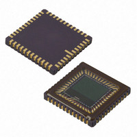
Manufacturer Part Number
MT9T031C12STC
Description
IC SENSOR IMAGE COLOR 48CLCC
Manufacturer
Aptina LLC
Series
Micron®DigitalClarity®r
Type
CMOS Imagingr
Datasheets
1.MT9T031C12STCH_ES.pdf
(12 pages)
2.MT9T031C12STCH_ES.pdf
(2 pages)
3.MT9T031C12STC.pdf
(2 pages)
4.MT9T031C12STC.pdf
(46 pages)
Specifications of MT9T031C12STC
Pixel Size
3.2µm x 3.2µm
Active Pixel Array
2048H x 1536V
Frames Per Second
12 ~ 93
Voltage - Supply
3 V ~ 3.6 V
Package / Case
48-CLCC
Brief Features
Superior Low Light Performance, Programmable Controls, Low Dark Current, High Frame Rate
Supply Voltage Range
3V To 3.6V
Operating Temperature Range
0°C To +60°C
Ic Function
Digital Image Sensor
Lead Free Status / RoHS Status
Lead free / RoHS Compliant
For Use With
557-1450 - KIT HEAD BOARD FOR MT9T031557-1451 - KIT DEV FOR MT9T031
Lead Free Status / Rohs Status
Compliant
Other names
557-1452
Available stocks
Company
Part Number
Manufacturer
Quantity
Price

Part Number:
MT9T031C12STC
Manufacturer:
APTINA
Quantity:
20 000


Sequence
Bus Idle State
Start Bit
Stop Bit
Slave Address
Data Bit Transfer
PDF: 3682685119/Source: 9830567334
MT9T031_DS - Rev.E 5/11 EN
A typical read or write sequence begins by the master sending a start bit. After the start
bit, the master sends the slave device's 8-bit address. The last bit of the address deter-
mines if the request is a read or a write, where a “0” indicates a write and a “1” indicates
a read. The slave device acknowledges its address by sending an acknowledge bit back to
the master.
If the request was a write, the master then transfers the 8-bit register address to which a
write should take place. The slave sends an acknowledge bit to indicate that the register
address has been received. The master then transfers the data eight bits at a time, with
the slave sending an acknowledge bit after each eight bits. The MT9T031 uses 16-bit data
for its internal registers, thus requiring two 8-bit transfers to write to one register. After
16 bits are transferred, the register address is automatically incremented, so that the next
16 bits are written to the next register address. The master stops writing by sending a
start or stop bit.
A typical read sequence is executed as follows. First the master sends the write-mode
slave address and 8-bit register address, just as in the write request. The master then
sends a start bit and the read-mode slave address. The master then clocks out the
register data eight bits at a time. The master sends an acknowledge bit after each 8-bit
transfer. The register address is auto-incremented after every 16 bits is transferred. The
data transfer is stopped when the master sends a no-acknowledge bit.
The bus is idle when both the data and clock lines are HIGH. Control of the bus is initi-
ated with a start bit, and the bus is released with a stop bit. Only the master can generate
the start and stop bits.
The start bit is defined as a HIGH-to-LOW transition of the data line while the clock line
is HIGH.
The stop bit is defined as a LOW-to-HIGH transition of the data line while the clock line
is HIGH.
The eight-bit address of a two-wire serial interface device consists of seven bits of
address and 1 bit of direction. A “0” (0xBA) in the LSB (least significant bit) of the address
indicates write mode, and a “1” (0xBB) indicates read mode.
One data bit is transferred during each clock pulse. The serial interface clock pulse is
provided by the master. The data must be stable during the HIGH period of the two-wire
serial interface clock—it can only change when the serial clock is LOW. Data is trans-
ferred eight bits at a time, followed by an acknowledge bit.
37
MT9T031: 1/2-Inch 3-Mp Digital Image Sensor
©2006 Aptina Imaging Corporation. All rights reserved.
Serial Bus Description
Related parts for MT9T031C12STC
Image
Part Number
Description
Manufacturer
Datasheet
Request
R

Part Number:
Description:
SENSOR IMAGE VGA COLOR CMOS PLCC
Manufacturer:
Aptina LLC
Datasheet:

Part Number:
Description:
SENSOR IMAGE 1.3MP CMOS 48-CLCC
Manufacturer:
Aptina LLC
Datasheet:

Part Number:
Description:
SENSOR IMAGE 2MP CMOS 48-CLCC
Manufacturer:
Aptina LLC
Datasheet:

Part Number:
Description:
SENSOR IMAGE VGA MONO 52IBGA
Manufacturer:
Aptina LLC
Datasheet:

Part Number:
Description:
SENSOR IMAGE VGA COLOR 48CLCC
Manufacturer:
Aptina LLC
Datasheet:

Part Number:
Description:
SENSOR IMAGE COLOR CMOS 48-PLCC
Manufacturer:
Aptina LLC
Datasheet:

Part Number:
Description:
KIT HEAD BOARD FOR MT9P031
Manufacturer:
Aptina LLC
Datasheet:

Part Number:
Description:
KIT HEAD BOARD FOR MT9D131
Manufacturer:
Aptina LLC
Datasheet:

Part Number:
Description:
KIT HEAD BOARD FOR MT9P031
Manufacturer:
Aptina LLC
Datasheet:

Part Number:
Description:
KIT HEAD BOARD FOR MT9M032
Manufacturer:
Aptina LLC
Datasheet:

Part Number:
Description:
PARALLEL HEADBOARD FOR MT9M032
Manufacturer:
Aptina LLC
Datasheet:
Part Number:
Description:
SENSOR IMAGE VGA COLOR CMOS PLCC
Manufacturer:
Aptina LLC
Datasheet:
Part Number:
Description:
SENSOR IMAGE 2MP CMOS 48-CLCC
Manufacturer:
Aptina LLC
Datasheet:
