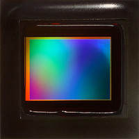
MT9P031I12STM Aptina LLC, MT9P031I12STM Datasheet - Page 9

MT9P031I12STM
Manufacturer Part Number
MT9P031I12STM
Description
SENSOR IMAGE 5MP MONO CMOS 48LCC
Manufacturer
Aptina LLC
Type
CMOS Imagingr
Datasheets
1.MT9P031I12STCH_ES.pdf
(12 pages)
2.MT9P031I12STCH_ES.pdf
(2 pages)
3.MT9P031I12STM.pdf
(12 pages)
Specifications of MT9P031I12STM
Package / Case
48-iLCC
Pixel Size
2.2µm x 2.2µm
Active Pixel Array
2592H x 1944V
Frames Per Second
60
Voltage - Supply
2.6 V ~ 3.1 V
Supply Voltage Range
1.7V To 3.1V, 1.7V To 1.9V, 2.6V To 3.1V
Operating Temperature Range
-30°C To +70°C
Digital Ic Case Style
PLCC
No. Of Pins
48
Supply Voltage Max
3.1V
Ic Function
Digital Image Sensor
Rohs Compliant
Yes
Lead Free Status / RoHS Status
Lead free / RoHS Compliant
For Use With
557-1430 - KIT HEAD BOARD FOR MT9P031557-1429 - KIT DEV FOR MT9P031
Lead Free Status / RoHS Status
Lead free / RoHS Compliant, Lead free / RoHS Compliant
Other names
557-1397
Q3884047
Q3956538
Q4007187
Q3884047
Q3956538
Q4007187
Available stocks
Company
Part Number
Manufacturer
Quantity
Price
Company:
Part Number:
MT9P031I12STM
Manufacturer:
ADI
Quantity:
119
Part Number:
MT9P031I12STM
Manufacturer:
APTINA
Quantity:
20 000
Company:
Part Number:
MT9P031I12STM-DP
Manufacturer:
ON
Quantity:
210
Company:
Part Number:
MT9P031I12STMD ES
Manufacturer:
Aptina LLC
Quantity:
135
Readout Modes
Subsampling
Skipping
Binning
PDF: 09005aef824c993e/Source: 09005aef824c9943
MT9P031_5100_PB_2.fm - Rev. B 8/07 EN
By default, the resolution of the output image is the full width and height of the FOV as
defined above. The output resolution can be reduced by two methods: skipping and bin-
ning.
Row and column skip modes use subsampling to reduce the output resolution without
reducing field-of-view. The MT9P031 also has row and column binning modes, which
can reduce the impact of aliasing introduced by the use of skip modes. This is achieved
by the averaging of two or three adjacent rows and columns (adjacent same-color pix-
els). Both 2X and 4X binning modes are supported. Rows and columns can be binned
independently.
Skipping reduces resolution by using only selected pixels from the FOV in the output
image. In skip mode, entire rows and columns of pixels are not sampled, resulting in a
lower-resolution output image. A skip 2X mode skips one Bayer pair of pixels for every
pair output. Skip 3X skips two pairs for each one pair output. Rows and columns are
always read out in pairs.
Binning reduces resolution by combining adjacent, same-color imager pixels to produce
one output pixel. All of the pixels in the FOV contribute to the output image in bin mode.
This can result in a more pleasing output image with reduced subsampling artifacts. It
also improves low-light performance. For columns, the combination step can be either
an averaging or summing operation. Depending on lighting conditions, one or the other
may be desirable. In low-light conditions, summing produces a gain roughly equivalent
to the column bin factor.
Only certain combinations of binning and skipping are allowed.
MT9P031: 1/2.5-Inch 5-Mp Digital Image Sensor
9
Micron Technology, Inc., reserves the right to change products or specifications without notice.
Functional Overview
©2006 Micron Technology, Inc. All rights reserved.


