MT9M001C12STM Aptina LLC, MT9M001C12STM Datasheet - Page 10
MT9M001C12STM
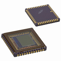
Manufacturer Part Number
MT9M001C12STM
Description
SENSOR IMAGE MONO CMOS 48-LCC
Manufacturer
Aptina LLC
Type
CMOS Imagingr
Datasheets
1.MT9M001C12STM.pdf
(35 pages)
2.MT9M001C12STM.pdf
(2 pages)
3.MT9M001C12STM.pdf
(28 pages)
Specifications of MT9M001C12STM
Pixel Size
5.2µm x 5.2µm
Active Pixel Array
1280H x 1024V
Frames Per Second
30
Voltage - Supply
3 V ~ 3.6 V
Package / Case
48-CLCC
Sensor Image Color Type
Monochrome
Sensor Image Size
1280x1024Pixels
Operating Supply Voltage (min)
3V
Operating Supply Voltage (typ)
3.3V
Operating Supply Voltage (max)
3.6V
Operating Temp Range
0C to 70C
Package Type
CLCC
Operating Temperature Classification
Commercial
Mounting
Surface Mount
Pin Count
48
Lead Free Status / RoHS Status
Lead free / RoHS Compliant
Other names
557-1151
Q3930625
Q3990821
Q3930625
Q3990821
Available stocks
Company
Part Number
Manufacturer
Quantity
Price
Company:

Part Number:
MT9M001C12STM
Manufacturer:
MICRON
Quantity:
1 000
Part Number:
MT9M001C12STM
Manufacturer:
MICRON/镁光
Quantity:
20 000


Frame Timing Formulas
Table 4:
Table 5:
PDF: 09005aef81c2856f/Source: 09005aef80a3e031
MT9M001_DS_2.fm - Rev. F 5/06 EN
Parameter
A
P
P
Q = P
A + Q
V
N
F
1
2
ROWS
Parameter
1
V’
F’
+ P
x (A + Q)
2
Frame Timing
Frame Time—Long Integration Time
Vertical Blanking (long integration time) (Reg0x09 – Reg0x03) x (A + Q)
Total Frame Time (long integration time) (Reg0x09 + 1) x (A + Q)
Active Data Time
Frame Start Blanking (242)
Frame End Blanking
Horizontal Blanking
Row Time
Vertical Blanking
Frame Valid Time
Total Frame Time
Notes:
Name
1. Row skip mode should have no effect on the integration time. Column skip mode changes
2. Default for Reg0x05 = 9. However, sensor ignores any value for Reg0x05 less than 19.
Sensor timing is shown above in terms of pixel clock and master clock cycles (please
refer to Figure 6). The recommended master clock frequency is 48 MHz. The vertical
blank and total frame time equations assume that the number of integration rows (bits
13 through 0 of Reg0x09) is less than the number of active plus blanking rows (Reg0x03 +
1 + Reg0x06 + 1). If this is not the case, the number of integration rows must be used
instead to determine the frame time, as shown in Table 5.
the effective value of Column Size (Reg0x04) as follows:
Column Skip 2 => R4eff = (int(R4 / 4) x 2) + 1
Column Skip 4 => R4eff = (int(R4 / 8) x 2) + 1
Column Skip 8 => R4eff = (int(R4 / 16) x 2) + 1
where the int() function truncates to the next lowest integer. Now use R4eff in the equa-
tion for row time instead of R4
Name
(Reg0x04 + 1)
(2 + Reg0x05 - 19)
(MIN Reg0x05 value = 19)
(244 + Reg0x05 - 19)
(MIN Reg0x05 value = 19)
((Reg0x04 + 1) + (244 + Reg0x05 - 19))
(Reg0x06 + 1) x (A + Q)
(MIN Reg0x06 value = 15)
(Reg0x03 + 1) x (A + Q)
(Reg0x03 + 1 + Reg0x06 + 1) x (A + Q)
Equation (MASTER CLOCK)
MT9M001: 1/2-Inch Megapixel Digital Image Sensor
10
Equation (master clock)
Micron Technology, Inc., reserves the right to change products or specifications without notice.
1,280 pixel clocks
= 26.7µs
242 pixel clocks
= 5.04µs
2 pixel clocks
= 0.042µs
244 pixel clocks
= 5.08µs
1,524 pixel clocks
= 31.75µs
39,624 pixel clocks
= 825.5µs
1,560,576 pixel clocks
= 32.51ms
1,600,200 pixel clocks
= 33.34ms
Default Timing
©2004 Micron Technology, Inc. All rights reserved.
Pixel Data Format
39,624 pixel clocks
= 82.5µs
1,600,200 pixel clocks
= 33.34ms
Default Timing
Notes
1
2
2
Related parts for MT9M001C12STM
Image
Part Number
Description
Manufacturer
Datasheet
Request
R

Part Number:
Description:
SENSOR IMAGE VGA COLOR CMOS PLCC
Manufacturer:
Aptina LLC
Datasheet:

Part Number:
Description:
IC SENSOR IMAGE COLOR 48CLCC
Manufacturer:
Aptina LLC
Datasheet:

Part Number:
Description:
SENSOR IMAGE 1.3MP CMOS 48-CLCC
Manufacturer:
Aptina LLC
Datasheet:

Part Number:
Description:
SENSOR IMAGE 2MP CMOS 48-CLCC
Manufacturer:
Aptina LLC
Datasheet:

Part Number:
Description:
SENSOR IMAGE VGA MONO 52IBGA
Manufacturer:
Aptina LLC
Datasheet:

Part Number:
Description:
SENSOR IMAGE VGA COLOR 48CLCC
Manufacturer:
Aptina LLC
Datasheet:

Part Number:
Description:
SENSOR IMAGE COLOR CMOS 48-PLCC
Manufacturer:
Aptina LLC
Datasheet:

Part Number:
Description:
KIT HEAD BOARD FOR MT9P031
Manufacturer:
Aptina LLC
Datasheet:

Part Number:
Description:
KIT HEAD BOARD FOR MT9D131
Manufacturer:
Aptina LLC
Datasheet:

Part Number:
Description:
KIT HEAD BOARD FOR MT9P031
Manufacturer:
Aptina LLC
Datasheet:
Part Number:
Description:
SENSOR IMAGE VGA COLOR CMOS PLCC
Manufacturer:
Aptina LLC
Datasheet:
Part Number:
Description:
IC SENSOR IMAGE COLOR 48CLCC
Manufacturer:
Aptina LLC
Datasheet:
Part Number:
Description:
SENSOR IMAGE 2MP CMOS 48-CLCC
Manufacturer:
Aptina LLC
Datasheet:
