2N5060 ON Semiconductor, 2N5060 Datasheet
2N5060
Specifications of 2N5060
Available stocks


Related parts for 2N5060

2N5060 Summary of contents
Page 1
... Low Holding Current − Maximum • Passivated Surface for Reliability and Uniformity • Device Marking: Device Type, e.g., 2N5060, Date Code • Pb−Free Packages are Available* *For additional information on our Pb−Free strategy and soldering details, please download the ON Semiconductor Soldering and Mounting Techniques Reference Manual, SOLDERRM/D. © ...
Page 2
... MAXIMUM RATINGS (T = 25°C unless otherwise noted) J Rating Peak Repetitive Off−State Voltage (Note *40 to 110°C, Sine Wave Hz kW) 2N5060 GK 2N5061 2N5062 2N5064 On-State Current RMS (180° Conduction Angles; T *Average On-State Current (180° Conduction Angles 67° 102°C) ...
Page 3
... T = 25° 110° 25° −40° 25° −40° 25° −40°C C 2N5060, 2N5061 2N5062, 2N5064 RRM RRM Reverse Blocking Region (off state) Reverse Avalanche Region Anode − http://onsemi.com 3 Symbol Min Typ Max DRM RRM − − 10 − − ...
Page 4
CONDUCTION ANGLE 120 110 100 30° 60° 0.1 0.2 0 AVERAGE ON‐STATE CURRENT (AMP) T(AV) Figure 1. Maximum Case Temperature 5.0 3.0 2 110°C J ...
Page 5
... TIME (SECONDS) Figure 6. Thermal Response TYPICAL CHARACTERISTICS 200 100 R = 100 1 5.0 2N5060‐61 2.0 1.0 0.5 0 100 110 -75 -50 2N5060,61 2N5062‐64 -50 - JUNCTION TEMPERATURE (°C) J Figure 9. Typical Holding Current http://onsemi.com 5 1.0 2 100 L 2N5062‐64 - JUNCTION TEMPERATURE (°C) J Figure 8 ...
Page 6
... ORDERING INFORMATION Device 2N5060 2N5060G 2N5060RLRA 2N5060RLRAG 2N5060RLRM 2N5060RLRMG 2N5061 2N5061G 2N5061RLRA 2N5061RLRAG 2N5062 2N5062G 2N5062RLRA 2N5062RLRAG 2N5064 2N5064RLRA 2N5064RLRM 2N5064RLRMG 2N5064RLRAG 2N5064G †For information on tape and reel specifications, including part orientation and tape sizes, please refer to our Tape and Reel Packaging Specifications Brochure, BRD8011/D ...
Page 7
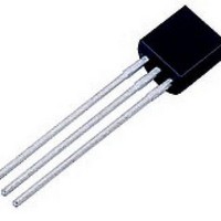
... B 4.32 5.33 C 3.18 4.19 D 0.40 0.54 G 2.40 2.80 J 0.39 0.50 K 12.70 --- N 2.04 2.66 P 1.50 4.00 R 2.93 --- V 3.43 --- STYLE 10: PIN 1. CATHODE 2. GATE 3. ANODE ON Semiconductor Website: www.onsemi.com Order Literature: http://www.onsemi.com/orderlit For additional information, please contact your local Sales Representative 2N5060/D ...