2N6344 ON Semiconductor, 2N6344 Datasheet

Triacs THY 8A 600V TRIAC

2N6344

Manufacturer Part Number
2N6344
Description
Triacs THY 8A 600V TRIAC
Manufacturer
ON Semiconductor
Datasheet

Specifications of 2N6344

Rated Repetitive Off-state Voltage Vdrm
600 V
Breakover Current Ibo Max
100 A
Off-state Leakage Current @ Vdrm Idrm
0.01 mA
Gate Trigger Voltage (vgt)
2 V
Gate Trigger Current (igt)
50 mA
Holding Current (ih Max)
40 mA
Forward Voltage Drop
1.55 V @ 11 A
Mounting Style
Through Hole
Package / Case
TO-220-3
Repetitive Peak Forward Blocking Voltage
600 V
Lead Free Status / RoHS Status
Lead free / RoHS Compliant

Available stocks

Company
Part Number
Manufacturer
Quantity
Price
Part Number:
2N6344
Manufacturer:
ON
Quantity:
1 000
Part Number:
2N6344AG
Manufacturer:
ON Semiconductor
Quantity:
1 928
Part Number:
2N6344G
Manufacturer:
ON
Quantity:
2 970
2N6344
Triacs
Silicon Bidirectional Thyristors
light dimmers, motor controls, heating controls and power supplies; or
wherever full−wave silicon gate controlled solid−state devices are
needed. Triac type thyristors switch from a blocking to a conducting
state for either polarity of applied main terminal voltage with positive
or negative gate triggering.
Features
Stresses exceeding Maximum Ratings may damage the device. Maximum
Ratings are stress ratings only. Functional operation above the Recommended
Operating Conditions is not implied. Extended exposure to stresses above the
Recommended Operating Conditions may affect device reliability.
†Indicates JEDEC Registered Data.
1. V
*For additional information on our Pb−Free strategy and soldering details, please
MAXIMUM RATINGS
May, 2006 − Rev. 4
†Peak Repetitive Off−State Voltage (Note 1)
(T
50 to 60 Hz, Gate Open)
†On−State RMS Current (T
Cycle Sine Wave 50 to 60 Hz (T
†Peak Non−Repetitive Surge Current (One
Full Cycle, Sine Wave 60 Hz, T
Preceded and followed by rated current
Circuit Fusing Consideration (t = 8.3 ms)
†Peak Gate Power
(T
†Average Gate Power
(T
†Peak Gate Current
(T
†Peak Gate Voltage
(T
†Operating Junction Temperature Range
Storage Temperature Range
download the ON Semiconductor Soldering and Mounting Techniques
Reference Manual, SOLDERRM/D.
Designed primarily for full-wave ac control applications, such as
Uniformity and Stability
Resistance, High Heat Dissipation and Durability
Blocking Voltage to 800 V
All Diffused and Glass Passivated Junctions for Greater Parameter
Small, Rugged, Thermowatt Construction for Low Thermal
Gate Triggering Guaranteed in all Four Quadrants
For 400 Hz Operation, Consult Factory
Pb−Free Package is Available*
Semiconductor Components Industries, LLC, 2006
voltages shall not be tested with a constant current source such that the
voltage ratings of the devices are exceeded.
J
C
C
C
C
DRM
= −40 to +110 C, Sine Wave
= +80 C, Pulse Width = 2 ms)
= +80 C, t = 8.3 ms)
= +80 C, Pulse Width = 2.0 ms)
and V
RRM
for all types can be applied on a continuous basis. Blocking
Rating
(T
J
C
= 25 C unless otherwise noted)
= +80 C) Full
Preferred Device
2N6344
2N6349
C
C
= +25 C)
= +90 C)
Symbol
I
P
V
V
T(RMS)
I
P
V
G(AV)
I
T
DRM,
TSM
RRM
I
GM
T
GM
GM
stg
2
J
t
−40 to +125
−40 to +150
Value
600
800
100
8.0
4.0
0.5
2.0
40
20
10
1
Unit
A
W
W
V
A
A
A
V
2
C
C
s
Preferred devices are recommended choices for future use
and best overall value.
2N6344
2N6344G
1
Device
2
1
2
3
4
3
MT2
ORDERING INFORMATION
600 thru 800 VOLTS
8 AMPERES RMS
A
Y
WW = Work Week
G
http://onsemi.com
PIN ASSIGNMENT
4
CASE 221A
TO−220AB
TO−220AB
TO−220AB
= Assembly Location
= Year
= Pb−Free Package
(Pb−Free)
Package
STYLE 4
TRIACS
Main Terminal 1
Main Terminal 2
Main Terminal 2
Publication Order Number:
Gate
500 Units / Box
500 Units / Box
MARKING
DIAGRAM
G
2N6344G
Shipping
AYWW
MT1
2N6344/D

Related parts for 2N6344

2N6344 Summary of contents

Page 1

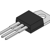
... Preferred devices are recommended choices for future use and best overall value. 1 http://onsemi.com TRIACS 8 AMPERES RMS 600 thru 800 VOLTS MT2 MT1 G MARKING DIAGRAM 4 2N6344G TO−220AB AYWW CASE 221A STYLE Assembly Location Y = Year WW = Work Week G = Pb−Free Package PIN ASSIGNMENT ...

Page 2

... Rise Time = 0.1 ms, Pulse Width = 2 ms Rated DRM TM GT DYNAMIC CHARACTERISTICS Critical Rate of Rise of Commutation Voltage (V = Rated Commutating di/dt = 4.0 A/ms, Gate Unenergized DRM TM †Indicates JEDEC Registered Data. 2N6344 ( unless otherwise noted; Electricals apply in both directions 100 100 Vdc 2N6349 only 2N6349 only = 100 Vdc ...

Page 3

... I − GT Quadrant III (−) I GATE Both All polarities are referenced to MT1. With in−phase signals (using standard AC lines) quadrants I and III are used. 2N6344 (Bidirectional Device) on state RRM RRM Quadrant 3 MainTerminal 2 − Quadrant Definitions for a Triac MT2 POSITIVE (Positive Half Cycle) ...

Page 4

... OFF-STATE VOLTAGE = 12 V 1.6 1.4 QUADRANT 4 1.2 1.0 0.8 1 QUADRANTS 2 0.6 3 0.4 −60 −40 − JUNCTION TEMPERATURE ( C) J Figure 3. Typical Gate Trigger Voltage 2N6344 CONDUCTION ANGLE 120 6.0 [ 100 180 4.0 2 6.0 7.0 8.0 0 1.0 Figure 2. On−State Power Dissipation 50 30 ...

Page 5

... INSTANTANEOUS ON-STATE VOLTAGE (VOLTS) TM Figure 5. On−State Characteristics 1.0 0.5 0.2 0.1 0.05 0.02 0.01 0.1 0.2 0.5 1.0 2.0 2N6344 20 10 7.0 5.0 3.0 2.0 −60 −40 −20 Figure 6. Typical Holding Current 100 80 60 CYCLE 100 ...

Page 6

... Z −−− 0.080 −−− 2.04 STYLE 4: PIN 1. MAIN TERMINAL 1 2. MAIN TERMINAL 2 3. GATE 4. MAIN TERMINAL 2 ON Semiconductor Website: www.onsemi.com Order Literature: http://www.onsemi.com/orderlit For additional information, please contact your local Sales Representative 2N6344/D ...

Related keywords