MBRF20100CTG ON Semiconductor, MBRF20100CTG Datasheet - Page 2
MBRF20100CTG
Manufacturer Part Number
MBRF20100CTG
Description
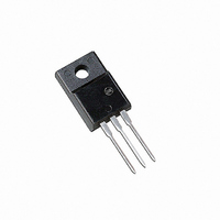
DIODE SCHOTTKY 100V 10A TO220FP
Manufacturer
ON Semiconductor
Series
SWITCHMODE™r
Datasheet
1.MBRF20100CTG.pdf
(4 pages)
Specifications of MBRF20100CTG
Voltage - Forward (vf) (max) @ If
850mV @ 10A
Current - Reverse Leakage @ Vr
150µA @ 100V
Current - Average Rectified (io) (per Diode)
10A
Voltage - Dc Reverse (vr) (max)
100V
Diode Type
Schottky
Speed
Fast Recovery =< 500ns, > 200mA (Io)
Diode Configuration
1 Pair Common Cathode
Mounting Type
Through Hole
Package / Case
TO-220-3 Full Pack (Straight Leads)
Rectifier Type
Schottky Diode
Configuration
Dual Common Cathode
Peak Rep Rev Volt
100V
Avg. Forward Curr (max)
20A
Rev Curr
150uA
Peak Non-repetitive Surge Current (max)
150A
Forward Voltage
0.95V
Operating Temp Range
-65C to 175C
Package Type
TO-220 Full-Pak
Operating Temperature Classification
Military
Mounting
Through Hole
Pin Count
3 +Tab
Lead Free Status / RoHS Status
Lead free / RoHS Compliant
Reverse Recovery Time (trr)
-
Lead Free Status / Rohs Status
Compliant
Other names
MBRF20100CTGOS
Available stocks
Company
Part Number
Manufacturer
Quantity
Price
Company:

Part Number:
MBRF20100CTG
Manufacturer:
ON
Quantity:
1 250
Company:
Part Number:
MBRF20100CTG
Manufacturer:
ON Semiconductor
Quantity:
1 850
Company:
Part Number:
MBRF20100CTG
Manufacturer:
ON
Quantity:
16
Part Number:
MBRF20100CTG
Manufacturer:
ON/安森美
Quantity:
20 000


Stresses exceeding Maximum Ratings may damage the device. Maximum Ratings are stress ratings only. Functional operation above the
Recommended Operating Conditions is not implied. Extended exposure to stresses above the Recommended Operating Conditions may affect
device reliability.
1. The heat generated must be less than the thermal conductivity from Junction-to-Ambient: dP
2. Proper strike and creepage distance must be provided.
3. Pulse Test: Pulse Width = 300 ms, Duty Cycle ≤ 2.0%.
MAXIMUM RATINGS
THERMAL CHARACTERISTICS
ELECTRICAL CHARACTERISTICS
Peak Repetitive Reverse Voltage
Average Rectified Forward Current
Peak Repetitive Forward Current
Non-repetitive Peak Surge Current
Peak Repetitive Reverse Surge Current (2.0 ms, 1.0 kHz)
Operating Junction and Storage Temperature Range (Note 1)
Voltage Rate of Change (Rated V
RMS Isolation Voltage (t = 0.3 second, R.H. ≤ 30%, T
Maximum Thermal Resistance, Junction to Case
Lead Temperature for Soldering Purposes: 1/8″ from Case for 5 Seconds
Maximum Instantaneous Forward Voltage (Note 3)
Maximum Instantaneous Reverse Current (Note 3)
5.0
3.0
1.0
0.5
50
20
10
(Rated V
(Rated V
(Surge applied at rated load conditions halfwave, single phase, 60 Hz)
(i
(i
(i
(i
(Rated DC Voltage, T
(Rated DC Voltage, T
F
F
F
F
0
Working Peak Reverse Voltage
DC Blocking Voltage
= 10 Amp, T
= 10 Amp, T
= 20 Amp, T
= 20 Amp, T
Figure 1. Typical Forward Voltage Per Diode
0.1
R
R
), T
, Square Wave, 20 kHz), T
0.2
C
v
C
C
C
C
= 133°C
F
, INSTANTANEOUS VOLTAGE (VOLTS)
= 25°C)
= 125°C)
= 25°C)
= 125°C)
0.3
(Per Leg)
C
C
= 25°C)
= 125°C)
0.4
150°C
R
0.5
)
(Per Leg)
Characteristic
C
(Per Leg)
0.6
= 133°C
Rating
Rating
0.7
T
J
100°C
= 25°C
0.8
A
= 25°C) (Note 2)
http://onsemi.com
MBRF20100CT
0.9
1.0
2
0.01
1.0
0.1
10
0
Total Device
Figure 2. Typical Reverse Current Per Diode
Per Figure 3
20
T
T
T
J
J
J
= 150°C
= 125°C
= 100°C
T
J
= 25°C
40
V
R
, REVERSE VOLTAGE (VOLTS)
D
/dT
Symbol
Symbol
Symbol
T
V
V
I
I
dv/dt
V
R
I
I
J
F(AV)
FRM
RRM
RWM
FSM
J
RRM
V
, T
T
v
iso1
i
qJC
60
R
R
F
< 1/R
L
stg
qJA
80
.
- 65 to +175
10000
Value
Value
4500
Max
0.85
0.75
0.95
0.85
0.15
100
150
260
150
0.5
3.5
10
20
20
100
120
°C/W
V/ms
Unit
Unit
Unit
mA
°C
°C
V
A
A
A
A
V
V
Related parts for MBRF20100CTG
Image
Part Number
Description
Manufacturer
Datasheet
Request
R

Part Number:
Description:
ON Semiconductor [VOLTAGE REGULATOR]
Manufacturer:
ON Semiconductor
Datasheet:
Part Number:
Description:
357-036-542-201 CARDEDGE 36POS DL .156 BLK LOPRO
Manufacturer:
ON Semiconductor
Datasheet:
Part Number:
Description:
357-036-542-201 CARDEDGE 36POS DL .156 BLK LOPRO
Manufacturer:
ON Semiconductor
Datasheet:
Part Number:
Description:
357-036-542-201 CARDEDGE 36POS DL .156 BLK LOPRO
Manufacturer:
ON Semiconductor
Datasheet:
Part Number:
Description:
357-036-542-201 CARDEDGE 36POS DL .156 BLK LOPRO
Manufacturer:
ON Semiconductor
Datasheet:
Part Number:
Description:
357-036-542-201 CARDEDGE 36POS DL .156 BLK LOPRO
Manufacturer:
ON Semiconductor
Datasheet:
Part Number:
Description:
357-036-542-201 CARDEDGE 36POS DL .156 BLK LOPRO
Manufacturer:
ON Semiconductor
Datasheet:
Part Number:
Description:
357-036-542-201 CARDEDGE 36POS DL .156 BLK LOPRO
Manufacturer:
ON Semiconductor
Datasheet:
Part Number:
Description:
357-036-542-201 CARDEDGE 36POS DL .156 BLK LOPRO
Manufacturer:
ON Semiconductor
Datasheet:
Part Number:
Description:
357-036-542-201 CARDEDGE 36POS DL .156 BLK LOPRO
Manufacturer:
ON Semiconductor
Datasheet:
Part Number:
Description:
357-036-542-201 CARDEDGE 36POS DL .156 BLK LOPRO
Manufacturer:
ON Semiconductor
Datasheet:
Part Number:
Description:
Manufacturer:
ON Semiconductor
Datasheet:
Part Number:
Description:
Manufacturer:
ON Semiconductor
Datasheet:
Part Number:
Description:
Manufacturer:
ON Semiconductor
Datasheet: